Metallic carbon circuit element enables work on faster, efficient carbon-based transistors
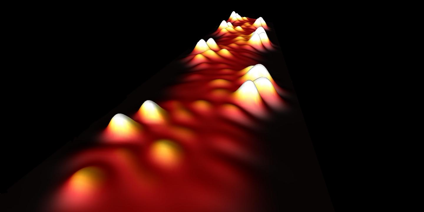
Credit: UC Berkeley image by Daniel Rizzo
Transistors based on carbon rather than silicon could potentially boost computers’ speed and cut their power consumption more than a thousandfold — think of a mobile phone that holds its charge for months — but the set of tools needed to build working carbon circuits has remained incomplete until now.
A team of chemists and physicists at the University of California, Berkeley, has finally created the last tool in the toolbox, a metallic wire made entirely of carbon, setting the stage for a ramp-up in research to build carbon-based transistors and, ultimately, computers.
“Staying within the same material, within the realm of carbon-based materials, is what brings this technology together now,” said Felix Fischer, UC Berkeley professor of chemistry, noting that the ability to make all circuit elements from the same material makes fabrication easier. “That has been one of the key things that has been missing in the big picture of an all-carbon-based integrated circuit architecture.”
Metal wires — like the metallic channels used to connect transistors in a computer chip — carry electricity from device to device and interconnect the semiconducting elements within transistors, the building blocks of computers.
The UC Berkeley group has been working for several years on how to make semiconductors and insulators from graphene nanoribbons, which are narrow, one-dimensional strips of atom-thick graphene, a structure composed entirely of carbon atoms arranged in an interconnected hexagonal pattern resembling chicken wire.
The new carbon-based metal is also a graphene nanoribbon, but designed with an eye toward conducting electrons between semiconducting nanoribbons in all-carbon transistors. The metallic nanoribbons were built by assembling them from smaller identical building blocks: a bottom-up approach, said Fischer’s colleague, Michael Crommie, a UC Berkeley professor of physics. Each building block contributes an electron that can flow freely along the nanoribbon.
While other carbon-based materials — like extended 2D sheets of graphene and carbon nanotubes — can be metallic, they have their problems. Reshaping a 2D sheet of graphene into nanometer scale strips, for example, spontaneously turns them into semiconductors, or even insulators. Carbon nanotubes, which are excellent conductors, cannot be prepared with the same precision and reproducibility in large quantities as nanoribbons.
“Nanoribbons allow us to chemically access a wide range of structures using bottom-up fabrication, something not yet possible with nanotubes,” Crommie said. “This has allowed us to basically stitch electrons together to create a metallic nanoribbon, something not done before. This is one of the grand challenges in the area of graphene nanoribbon technology and why we are so excited about it.”
Metallic graphene nanoribbons — which feature a wide, partially-filled electronic band characteristic of metals — should be comparable in conductance to 2D graphene itself.
“We think that the metallic wires are really a breakthrough; it is the first time that we can intentionally create an ultra-narrow metallic conductor — a good, intrinsic conductor — out of carbon-based materials, without the need for external doping,” Fischer added.
Crommie, Fischer and their colleagues at UC Berkeley and Lawrence Berkeley National Laboratory (Berkeley Lab) will publish their findings in the Sept. 25 issue of the journal Science.
Tweaking the topology
Silicon-based integrated circuits have powered computers for decades with ever increasing speed and performance, per Moore’s Law, but they are reaching their speed limit — that is, how fast they can switch between zeros and ones. It’s also becoming harder to reduce power consumption; computers already use a substantial fraction of the world’s energy production. Carbon-based computers could potentially switch many times times faster than silicon computers and use only fractions of the power, Fischer said.
Graphene, which is pure carbon, is a leading contender for these next-generation, carbon-based computers. Narrow strips of graphene are primarily semiconductors, however, and the challenge has been to make them also work as insulators and metals — opposite extremes, totally nonconducting and fully conducting, respectively — so as to construct transistors and processors entirely from carbon.
Several years ago, Fischer and Crommie teamed up with theoretical materials scientist Steven Louie, a UC Berkeley professor of physics, to discover new ways of connecting small lengths of nanoribbon to reliably create the full gamut of conducting properties.
Two years ago, the team demonstrated that by connecting short segments of nanoribbon in the right way, electrons in each segment could be arranged to create a new topological state — a special quantum wave function — leading to tunable semiconducting properties.
In the new work, they use a similar technique to stitch together short segments of nanoribbons to create a conducting metal wire tens of nanometers long and barely a nanometer wide.
The nanoribbons were created chemically and imaged on very flat surfaces using a scanning tunneling microscope. Simple heat was used to induce the molecules to chemically react and join together in just the right way. Fischer compares the assembly of daisy-chained building blocks to a set of Legos, but Legos designed to fit at the atomic scale.
“They are all precisely engineered so that there is only one way they can fit together. It’s as if you take a bag of Legos, and you shake it, and out comes a fully assembled car,” he said. “That is the magic of controlling the self-assembly with chemistry.”
Once assembled, the new nanoribbon’s electronic state was a metal — just as Louie predicted — with each segment contributing a single conducting electron.
The final breakthrough can be attributed to a minute change in the nanoribbon structure.
“Using chemistry, we created a tiny change, a change in just one chemical bond per about every 100 atoms, but which increased the metallicity of the nanoribbon by a factor of 20, and that is important, from a practical point of view, to make this a good metal,” Crommie said.
The two researchers are working with electrical engineers at UC Berkeley to assemble their toolbox of semiconducting, insulating and metallic graphene nanoribbons into working transistors.
“I believe this technology will revolutionize how we build integrated circuits in the future,” Fischer said. “It should take us a big step up from the best performance that can be expected from silicon right now. We now have a path to access faster switching speeds at much lower power consumption. That is what is driving the push toward a carbon-based electronics semiconductor industry in the future.”
###
Co-lead authors of the paper are Daniel Rizzo and Jingwei Jiang from UC Berkeley’s Department of Physics and Gregory Veber from the Department of Chemistry. Other co-authors are Steven Louie, Ryan McCurdy, Ting Cao, Christopher Bronner and Ting Chen of UC Berkeley. Jiang, Cao, Louie, Fischer and Crommie are affiliated with Berkeley Lab, while Fischer and Crommie are members of the Kavli Energy NanoSciences Institute.
The research was supported by the Office of Naval Research, the Department of Energy, the Center for Energy Efficient Electronics Science and the National Science Foundation.
Media Contact
Robert Sanders
[email protected]


