
Credit: Ultrafast and Nanoscale Optics Group at UC San Diego
Engineers at the University of California San Diego have developed a material that could reduce signal losses in photonic devices. The advance has the potential to boost the efficiency of various light-based technologies including fiber optic communication systems, lasers and photovoltaics.
The discovery addresses one of the biggest challenges in the field of photonics: minimizing loss of optical (light-based) signals in devices known as plasmonic metamaterials.
Plasmonic metamaterials are materials engineered at the nanoscale to control light in unusual ways. They can be used to develop exotic devices ranging from invisibility cloaks to quantum computers. But a problem with metamaterials is that they typically contain metals that absorb energy from light and convert it into heat. As a result, part of the optical signal gets wasted, lowering the efficiency.
In a recent study published in Nature Communications, a team of photonics researchers led by electrical engineering professor Shaya Fainman at the UC San Diego Jacobs School of Engineering demonstrated a way to make up for these losses by incorporating into the metamaterial something that emits light — a semiconductor.
"We're offsetting the loss introduced by the metal with gain from the semiconductor. This combination theoretically could result in zero net absorption of the signal — a 'lossless' metamaterial," said Joseph Smalley, an electrical engineering postdoctoral scholar in Fainman's group and the first author of the study.
In their experiments, the researchers shined light from an infrared laser onto the metamaterial. They found that depending on which way the light is polarized — which plane or direction (up and down, side to side) all the light waves are set to vibrate — the metamaterial either reflects or emits light.
"This is the first material that behaves simultaneously as a metal and a semiconductor. If light is polarized one way, the metamaterial reflects light like a metal, and when light is polarized the other way, the metamaterial absorbs and emits light of a different 'color' like a semiconductor," Smalley said.
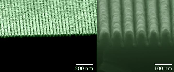
Researchers created the new metamaterial by first growing a crystal of the semiconductor material, called indium gallium arsenide phosphide, on a substrate. They then used high-energy ions from plasma to etch narrow trenches into the semiconductor, creating 40-nanometer-wide rows of semiconductor spaced 40 nanometers apart. Finally, they filled the trenches with silver to create a pattern of alternating nano-sized stripes of semiconductor and silver.
"This is a unique way to fabricate this kind of metamaterial," Smalley said. Nanostructures with different layers are often made by depositing each layer separately one on top of another, "like a stack of papers on a desk," Smalley explained. But the semiconductor material used in this study (indium gallium arsenide phosphide) can't just be grown on top of any substrate (like silver), otherwise it will have defects. "Rather than creating a stack of alternating layers, we figured out a way to arrange the materials side by side, like folders in a filing cabinet, keeping the semiconductor material defect-free."
As a next step, the team plans to investigate how much this metamaterial and other versions of it could improve photonic applications that currently suffer from signal losses.
###
###
Full paper: "Luminescent hyperbolic metasurfaces." Authors of the study are J.S.T. Smalley, F. Vallini, S.A. Montoya, L. Ferrari, S. Shahin, C.T. Riley, B. Kanté, E.E. Fullerton, Z. Liu and Y. Fainman.
This work was supported by the Office of Naval Research Multidisciplinary Research Initiative (N00014-13-1-0678), the National Science Foundation (ECE3972 and ECCS-1229677), the National Science Foundation Center for Integrated Access Networks (EEC-0812072), the Defense Advanced Research Projects Agency (N66001-12-1-4205) and the Cymer Corporation.
Media Contact
Liezel Labios
[email protected]
858-246-1124
@UCSanDiego
http://www.ucsd.edu
############
Story Source: Materials provided by Scienmag


