


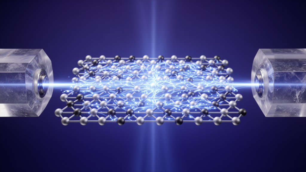
Experimental investigations into the two-dimensional Janus material tungsten selenium telluride, structurally formulated as WSeTe, have revealed an unexpected reversal in optoelectronic transport alongside structural stability under extreme mechanical loads. Researchers examining the compound inside diamond anvil cell apparatuses observed that positive photoconductivity under simulated solar illumination abruptly transforms into negative photoconductivity once hydrostatic pressure surpasses 1.4 gigapascals. Rather than triggering a destructive structural collapse or a crystalline phase transformation, mechanical compression drives intrinsic selenium-substituted tellurium point defects to evolve from shallow carrier transport paths into deep-level recombination centers. Across the broader loading regime extending up to 30 gigapascals, in situ Raman spectroscopy confirmed that the asymmetric layered lattice remains intact without symmetry breaking or lattice disintegration, demonstrating mechanical resilience under both quasi-hydrostatic pressure and applied rotational shear stress.
Janus transition metal dichalcogenides represent an unusual category of two-dimensional semiconductors where the inversion symmetry characteristic of conventional layered dichalcogenides is intentionally broken across the out-of-plane axis. In WSeTe, a central layer of tungsten atoms is bonded to selenium atoms across its top surface and tellurium atoms across its bottom surface. The significant differences in electronegativity and covalent radius between selenium and tellurium generate an intrinsic vertical dipole moment, a built-in out-of-plane electric field, and permanent internal strain. While earlier first-principles computational models predicted that WSeTe would retain semiconducting behavior under moderate hydrostatic pressures accompanied by continuous bandgap narrowing and enhanced optical absorption, direct experimental verification of its lattice dynamics, electronic transport, and defect evolution under severe multi-axial stress environments had remained unfulfilled prior to this systematic study.
To establish baseline material quality before diamond anvil cell loading, the research team carried out extensive phase and composition analyses on synthesized powder samples possessing 99.99 percent nominal purity. Powder X-ray diffraction patterns matched reference standards without secondary phase signatures, confirming high crystalline purity. Scanning electron microscopy showed irregular powder morphology, while energy-dispersive X-ray spectroscopy confirmed the presence and homogeneous spatial distribution of tungsten, selenium, and tellurium. Quantitative microanalysis yielded elemental concentrations of 35.63 atomic percent tungsten, 43.30 atomic percent selenium, and 21.07 atomic percent tellurium, establishing an experimental stoichiometry of approximately 1 to 1.21 to 0.61. Density functional theory calculations using plane-wave expansions and the generalized gradient approximation under the P63/mmc space group constraint complemented the experimental measurements by modeling vibrational mode assignments and dynamic stability.
High-pressure optical and electronic measurements were conducted using customized diamond anvil cell platforms, with shear stress specifically introduced through a rotational diamond anvil cell. Gasket preparation involved pre-indenting steel sheets to an initial thickness of 30 micrometers, drilling a central indentation of 180 micrometers, and backfilling the aperture with a composite mixture of boron nitride and epoxy resin before boring a final central sample chamber of 100 micrometers in diameter. Experiments were performed without a liquid pressure-transmitting medium to maintain direct mechanical coupling and shear application. In situ pressure was continuously calibrated through standard ruby fluorescence line shifts. Vibrational responses were collected under 532-nanometer laser excitation focused through a twenty-times objective to a one-micrometer spot, with scattered light resolved via a Horiba iHR550 spectrometer, while baseline corrections and Lorentzian deconvolution isolated individual phonon modes.
At ambient pressure, deconvolution of the experimental Raman spectra identified six distinct vibrational modes between 150 and 500 inverse centimeters, reflecting a composite dynamic character derived from binary tungsten diselenide and tungsten ditelluride parent lattices alongside newly induced Janus modes. Specifically, a mode near 180 inverse centimeters corresponds to parent telluride vibrations, while a peak at 220 inverse centimeters represents tellurium-tungsten out-of-plane stretching shifted by selenium incorporation. Two unique intermediate peaks at 200 and 230 inverse centimeters, designated as M1 and M2 modes, originate directly from local lattice distortions caused by disordered chalcogen distribution across the layer surfaces. High-frequency peaks located at 240 and 250 inverse centimeters correspond to coupled in-plane and out-of-plane sublayer vibrations. Mode calculations categorized these features into out-of-plane A1 stretching vibrations and in-plane E shear vibrations relative to the internal tungsten plane.
Upon quasi-hydrostatic compression up to 30 gigapascals, all six Raman modes exhibited continuous, monotonic blue shifts toward higher wavenumbers alongside linewidth broadening and intensity reduction, which are typical spectroscopic signatures of bond compression and increasing phonon frequencies. Throughout this entire compression trajectory, no Raman peaks split, vanished, or emerged anew, ruling out macroscopic crystal symmetry breaking or first-order structural reconstructive transitions. When rotational shear stress was deliberately introduced using the rotational anvil cell, the blue-shift rates of all six vibrational modes decreased systematically compared to quasi-hydrostatic compression. Linear fits of mode frequencies against pressure revealed that shear stress decreased the first-order pressure coefficients by an average of 17.7 percent, dropping from initial values between 1.13 and 1.46 inverse centimeters per gigapascal down to values between 0.91 and 1.34 inverse centimeters per gigapascal.
This uniform dampening of Raman pressure coefficients under shear reflects lattice anharmonicity and microscopic strain heterogeneity within the asymmetric crystal. Rotational deformation introduces non-hydrostatic shear components that disrupt purely volumetric compression, altering bond angles and interatomic distances in ways that soften mode Grüneisen parameters. Modes exhibited distinct localized sensitivities to shear: the out-of-plane vibration at 250 inverse centimeters underwent the largest suppression in its pressure coefficient, demonstrating that vibrations involving vertical chalcogen displacement are especially sensitive to interlayer sliding forces and local stacking modifications. Conversely, the intralayer mode at 200 inverse centimeters showed the smallest coefficient reduction, indicating that rigid in-plane atomic bonds provide superior mechanical resistance against shear disorder. Upon full decompression, all Raman frequencies returned to their starting positions, confirming the structural reversibility of the compressed lattice despite slight residual line broadening from microstrain.
The exceptional resistance of WSeTe against shear-induced phase transformation stands in sharp contrast to conventional transition metal dichalcogenides, which frequently undergo structural phase transitions via low-barrier interlayer sliding. In Janus WSeTe, the vertical asymmetry between top selenium and bottom tellurium layers generates an uneven charge distribution, creating a persistent built-in electric field and interlayer dipole moment. As external pressure compresses the van der Waals gap between adjacent sheets, electronic orbital wavefunctions overlap more extensively across the interlayer space. This increased hybridization elevates both the interlayer shear modulus and the kinetic barrier opposing relative lateral displacement. Consequently, the combined stabilizing effects of dipole-assisted coupling and orbital overlap prevent shear forces from initiating the layer-sliding pathways that typically trigger structural reconstruction in layered chalcogenide crystals.
While the crystal framework remained structurally invariant, in situ electrical transport measurements conducted under 500 milliwatt per square centimeter xenon lamp illumination revealed drastic, anomalous transformations in optoelectronic response. At a modest pressure of 0.4 gigapascals, WSeTe displayed conventional positive photoconductivity, in which illumination generates free electron-hole pairs that elevate the total mobile carrier density and lower material resistance. However, once applied pressure surpassed 1.4 gigapascals, the sign of the photoresponse inverted entirely into negative photoconductivity, where steady illumination reduced the measurable current. Because Raman diagnostics excluded crystalline phase changes, this functional inversion was traced to the local electronic structure of intrinsic selenium-substituted-tellurium point defects, which density functional modeling identifies as the most thermodynamically stable native defect configuration within the compound.
Under mild compression below 1.4 gigapascals, selenium-substituted-tellurium defects occupy shallow energy levels within the electronic bandgap, facilitating the spatial separation and transport of photogenerated charge carriers. As pressure exceeds 1.4 gigapascals, shrinking interatomic distances strengthen local orbital hybridization around these point defect sites, driving an orbital reconstruction that shifts the localized defect states deeper into the forbidden band toward the Fermi level. This pressure-driven transition parallels the mechanism of the anti-Wilson effect by altering local orbital interactions, but specifically modulates localized mid-gap states rather than shifting global band edges. Once positioned as deep-level recombination centers, these transformed defects strongly capture photogenerated electrons and holes, facilitating rapid non-radiative recombination and generating charged scattering centers that suppress both free-carrier concentrations and carrier mobilities under light.
Simultaneous electrical resistivity monitoring revealed another set of electronic anomalies during compression: sharp, discontinuous, step-like resistance jumps occurring at 6.9, 15.0, and 19.1 gigapascals. Following each jump, the resistance-pressure curve resumed its original slope, signifying that the underlying electronic parent framework remained intact. The authors systematically eliminated alternative electronic explanations, noting that Lifshitz transitions produce smooth resistance extrema rather than discrete vertical steps, while excitonic condensation requires low temperatures incompatible with these room-temperature observations. Instead, the multi-step jumps were identified as sequential orbital-selective Mott transitions. The intrinsic out-of-plane asymmetry and structural strain gradients generate a non-uniform microscopic strain field across the tungsten d orbitals, causing their respective ratios of on-site Coulomb repulsion to electronic bandwidth to evolve at different rates until individual orbitals sequentially undergo Mott localization.
Decompression measurements further demonstrated that the pressure-altered electronic ground state possesses pronounced non-volatile memory and first-order kinetic characteristics. Throughout pressure release, WSeTe continuously retained negative photoconductivity down to ambient levels, confirming that the transformation of point defects into deep-level recombination centers is kinetically protected by a substantial energy barrier related to local bond distortions and lattice strain. In parallel, the electrical resistance displayed prominent hysteresis: the resistance jump observed at 15.0 gigapascals during compression re-emerged at 13.4 gigapascals during decompression, accompanied by asymmetric resistance trajectories between 16.8 and 30 gigapascals. This non-coincidence of forward and backward transport paths confirms that strong electron-lattice coupling stabilizes metastable electronic configurations under load, offering fundamental insights into the non-volatile manipulation of low-dimensional optoelectronics in extreme mechanical environments.
Subject of Research: High-pressure lattice dynamics, orbital-selective Mott transitions, and defect-driven negative photoconductivity in Janus WSeTe
Article Title: Lattice response and anomalous photoconductivity in Janus WSeTe under high pressure and shear stress
Article References: Liu, Q., Wang, Z., Cui, J., Guo, H., Wang, Q., Wang, G., Zhang, H., Zhang, G., Cao, Z., & Liu, C. (2026). Lattice response and anomalous photoconductivity in Janus WSeTe under high pressure and shear stress. Discover Nano, 21(1), Article 634. https://doi.org/10.1186/s11671-026-05067-7
Image Credits: AI Generated
DOI: 10.1186/s11671-026-05067-7
Keywords: Janus WSeTe, two-dimensional materials, diamond anvil cell, rotational diamond anvil cell, negative photoconductivity, positive photoconductivity, Raman spectroscopy, orbital-selective Mott transition, high pressure, shear stress, SeTe point defects, deep-level recombination centers, interlayer coupling, pressure coefficients, hysteresis, electrical transport, electronic correlation, xenon lamp illumination
News Source: Denise Maddox. (November 12, 2026). Janus Tungsten Selenium Telluride Develops Negative Photoconductivity Under Mild Compression. Scienmag.