Cu-Si alloy at high temperature offers clues for the synthesis of wafer-scale, single crystalline graphene stacking and for our lives after the end of the Moore’s Law
Credit: IBS
Graphene, an atomically thin hexagonal structure of carbon atoms is a potential candidate for electronic and optoelectrical applications such as transparent electrodes and interconnect for integrated circuits. Yet, it is one thing to possess such useful properties and to induce an intended characteristic from this “wonder material” is another. In the face of the end of the “Moore’s Law”, chip makers have set their sight on multi-layered graphene for its scaling ability of integrated circuits to smaller physical dimensions and the electric-field induced bandgap, which is not affordable in monolayer graphene. Furthermore, owning to exotic physical properties controlled by its stacking orders (the arrangement of graphene layer along vertical direction) such as superconductivity and quantum Hall effect to name a few, multi-layer graphene is an interesting material for condensed matter physicists. Still, the unknown growth method for uniform single-crystalline multilayer graphene growth in a wafer scale presents a challenge.
Led by professor LEE Young Hee at the Center for Integrated Nanostructure Physics, the Institute for Basic Science (IBS) in Sungkyunkwan University, South Korea, an IBS research team reports a novel method to grow multi-layered, single-crystalline graphene with a selected stacking order in a wafer scale. They obtained four-layered graphene using chemical vapor deposition (CVD) via Cu-Si alloy formation.
There have been several approaches to control the number of graphene layers. Conventionally, the monolayer graphene, which is easily grown on Cu-substrate, can be detached from the Cu-substrate and transferred onto insulator substrates such as SiO2/Si. Therefore, the simplest method to make multilayer graphene is to stack them layer-by-layer via the transfer process. However, this transfer process may cause tearing, wrinkles, and/or polymer residues. Though such issues can be avoided via a direct method, i.e. CVD on Cu substrate, the low solubility of carbon (C) in copper (Cu) hampers the controlling of the number of graphene layers with high uniformity in a large area. By depositing Ni or Co to form Cu-Ni/ Cu-Co alloys or employing oxygen-rich Cu substrate, C solubility in Cu is boosted and thus stacks more layers of graphene. Nevertheless, a small portion of inhomogeneous multilayers occurs. Controlling the crystallographic stacking sequence of graphene films thicker than two layers with high uniformity has not been demonstrated to date.
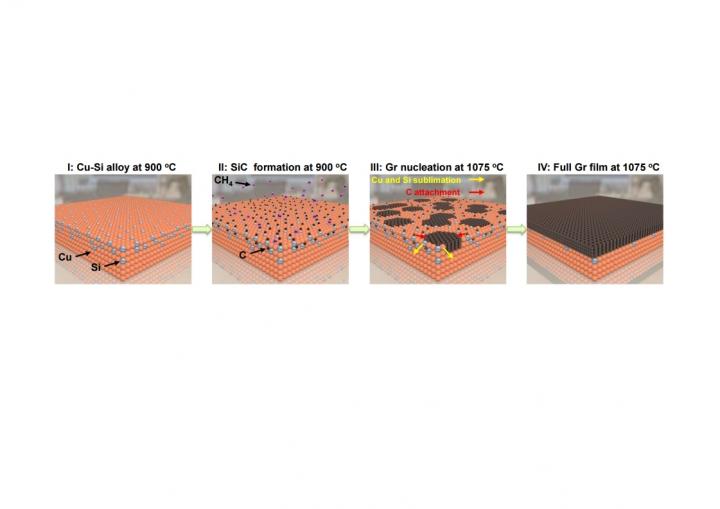
Dr. Van Luan Nguyen, the first author of the study (now at Samsung Advanced Institute Technology) proposed to use silicon carbide (SiC) on the surface of Cu substrate alloy, via the sublimation of Si atoms at a high temperature. They controlled the C solubility in the Cu film by introducing Si content on Cu surface by heat treatment of Cu substrate with a constant H2 gas flow inside the quartz tube of CVD chamber. “The formation of a homogeneous Cu-Si alloy, as a role of catalyst, was critical to control the number layers of graphene film in a wafer scale with methane gas. With the presence of Cu-Si alloy, SiC can be formed when methane gas is injected and the following sublimation process of Si atoms leaves C atoms behind to form multilayer graphene. Si amount is fixed at 28.7 % for uniform multilayer graphene film. Depending the concentrations of argon (Ar)-diluted methane gas, the number of graphene layers varies,” says Dr. Van.
Growing in a large scale of this much-hyped graphene has seen much progress over a decade, but building multi-layered graphene is just in its early stages. Our study offers a novel approach to upgrade the conventional CVD method by introducing an intermediate process of in-situ formation of SiC film,” notes Dr. LEE Sang Hyub, coauthor of the study. Importantly, this study provides a new platform to synthesize graphene multilayer towards the uniform large-area single-crystalline layer-tunable multilayer graphene as well as graphite thin film. This is an initial step to incorporate multilayer graphene to display panels and integrated circuits such as via-holes and replacement of Cu electrodes as well as photoelectronic and photovoltaic devices.
“Deposition of Si by conventional methods at low temperatures such as thermal evaporation or sputtering does not work for uniform multilayer graphene growth. The key in our new approach is to form uniform Cu-Si alloy on quartz tube chamber in which Si is sublimated at high temperature of 900 ? with H2 gas flow in a controllable manner,” explains Director LEE Young Hee, the corresponding author of the study. Although the substantial achievement has been demonstrated in our current work, Director Lee cautions that the method to deposit Si at high temperature during the growth process is not practical and can be harmful for the quart tube for long-term use. They are searching for a solution to replace the current one for mass product.
###
Media Contact
Sanghyub Lee
[email protected]
Related Journal Article
http://dx.


