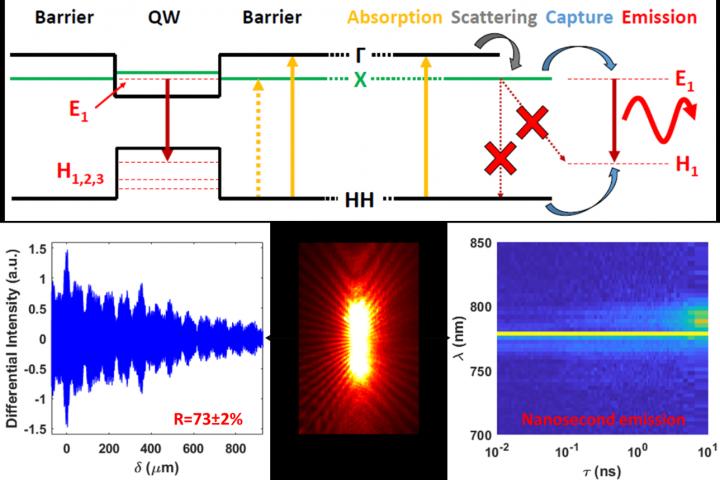
Credit: by Stefan Skalsky, Yunyan Zhang, Juan Arturo Alanis, H. Aruni Fonseka, Ana M. Sanchez, Huiyun Liu and Patrick Parkinson
Over the past decade, the idea of photonic computing – where electrons are replaced with light in microelectronic circuits – has emerged as a future technology. This promises low-cost, ultra-high-speed and potentially quantum-enhanced computing, with specific applications in high-efficiency machine learning and neuromorphic computing. While the computing elements and detectors have been developed, the need for nanoscale, high-density and easily-integrated light sources remains unmet. Semiconductor nanowires are seen as a potential candidate, due to their small size (on the order of the wavelength of light), the possibility for direct growth onto industry-standard silicon, and their use of established materials. However, to date, such nanowire lasers on silicon have not been demonstrated to operate continuously at room temperature.
In a new paper published in Light Science & Application, scientists from the Photon Science Institute in Manchester, UK with colleagues at University College London and the University of Warwick demonstrate a new route to achieving low-threshold silicon-integratable nanowire lasers. Based on a novel direct-indirect semiconductor heterostructures enabled by the nanowire platform, they demonstrate multi-nanosecond lasing at room temperature. A key design element is the need for high-reflectivity nanowire ends; this is typically a challenging requirement, as common growth methods do not allow simple optimization for high quality end-facets. However, in this study, by employing a novel time-gated interferometer the researchers demonstrate that the reflectivity can be over 70% – around double that expected for a conventional flat-ended laser due to the confinement of light.
Together, the novel material structure and high quality cavity contribute to a low lasing threshold – a measure of the power required to activate lasing in the nanowires – of just 6uJ/cm^2, orders of magnitude lower than previously demonstrated. Not only does this new approach provide high quality nanolasers, but the MBE growth provides a high-yield of functioning wires, with over 85% of nanowires tested working at full power without thermal damage. This high yield is critical for industrial integration of this new structure.
###
Media Contact
Patrick Parkinson
[email protected]
Related Journal Article
http://dx.


