Credit: by Wei Dai, Weikang Liu, Jian Yang, Chao Xu, Alessandro Alabastri, Chang Liu, Peter Nordlander, Zhiqiang Guan, and Hongxing Xu
Photoelectric conversion is an efficient and green way of energy conversion, which has important applications in light energy utilization and optical information devices. It is reported that up to 40% of the energy loss in the single-junction solar cells is due to the thermal loss of the carrier and the low light absorption of the device. The utilization of hot carrier energy in nanomaterials is the key to further improve the photoelectric conversion efficiency. Photothermoelectric effect is a photoelectric response driven by the gradient distribution of carrier temperature which is different from the lattice temperature. This effect has been reported in low dimensional nanomaterials, such as carbon nanotubes, III-V semiconductor nanowires, graphene, black phosphorus, and so on. Unfortunately, due to the low light absorption of low dimensional nanomaterials and the lack of high quality and reliable fabrication process, the photothermoelectric effect is still difficult to be applied in practical applications.
In a new paper published in Light Science & Application, a team of scientists, led by Academician Hongxing Xu and Associate Professor Zhiqiang Guan from School of Physics and Technology, Wuhan University, China, and co-workers have observed the giant photothermoelectric effect in the earth-abundant and CMOS compatible silicon nanomaterials. The photoelectric response of the photothermoelectric effect is 3-4 orders of magnitude higher than that reported previously, benefitting from the optimization process by the photo-thermal-electric multi-physics model with the carrier-lattice two-temperature model. It provides an important way for the practical application of photothermoelectric effect to improve photoelectric conversion efficiency by using hot carrier energy.
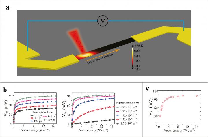
Photothermoelectric effect is a new type of photoelectric conversion mechanism, which uses the temperature gradient of photogenerated hot carriers to drive the directional movement of carriers and generate open-circuit voltage or short-circuit current photoelectric response. This effect usually occurs in low-dimensional nanomaterials due to the limited energy exchange between hot carriers and phonons by the suppressed phonon scattering and induces the carrier temperature different from the lattice temperature. Previous studies on hot carriers in silicon materials were mainly focused on the transient hot carrier temperature generated by short-pulse laser. The photothermoelectric effect based on the temperature distribution of steady hot carriers is rarely reported. These scientists summarized the reasons for the successful observation of giant photothermoelectric effects in silicon nanomaterials:
“The successful observation of photothermoelectric effect depends on ohmic electrode contact, appropriate doping concentration and size-limited carrier-phonon interaction. Ohmic electrode contact avoids the interference of the photovoltaic effect. The low doping concentration and the carrier-phonon interaction time up to 160 ps result in a stable temperature difference of 300K at the hot and cold end of the device and an open circuit photovoltage response of 105 V/W under 633 nm laser irradiation. The successful modeling of experimental results and the optimization of photothermoelectric effect by the photo-thermal-electric multi-physics model with the carrier-lattice two-temperature model are also the key to success.”
“It is very interesting to study the generation, relaxation and transportation of photogenerated carriers in nanomaterials. How to utilize the energy of hot carriers is a great challenge. Although the reported photothermoelectric effect in this paper faces the problems of slow speed and low energy filling ratio, we hope the further in-depth study of the photothermoelectric effect and the synergistic effect of photothermoelectric effect with other photoelectric conversion mechanisms such as photovoltaic effect and with the plasmon-enhanced light absorption, will finally break the limit of photoelectric conversion efficiency by using hot carrier energy.” they added.
###
Media Contact
Zhiqiang Guan
[email protected]
Related Journal Article
http://dx.


