Credit: Tokyo Tech
The electronic properties of solid materials are highly dependent on crystal structures and their dimensionalities (i.e., whether the crystals have predominantly 2D or 3D structures). As Professor Takayoshi Katase of Tokyo Institute of Technology notes, this fact has an important corollary: “If the crystal structure dimensionality can be switched reversibly in the same material, a drastic property change may be controllable.” This insight led Prof. Katase and his research team at Tokyo Institute of Technology, in partnership with collaborators at Osaka University and National Institute for Materials Science, to embark on research into the possibility of switching the crystal structure dimensionality of a lead-tin-selenide alloy semiconductor. Their results appear in a paper published in a recent issue of the peer-reviewed journal Science Advances.
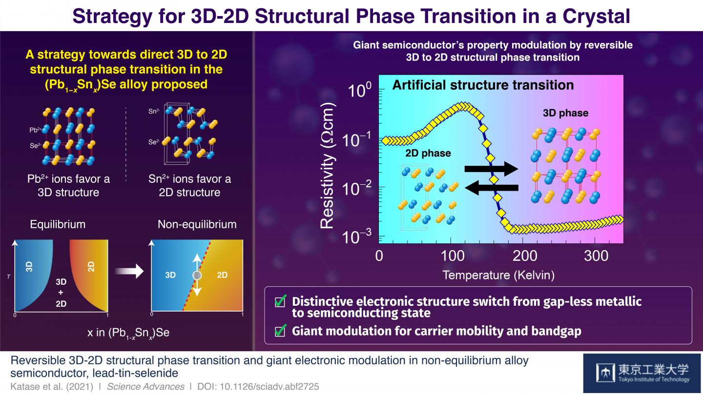
The lead-tin-selenide alloy, (Pb1?xSnx)Se is an appropriate focus for such research because the lead ions (Pb2+) and tin ions (Sn2+) favor distinct crystal dimensionalities. Specifically, pure lead selenide (PbSe) has a 3D crystal structure, whereas pure tin selenide (SnSe) has a 2D crystal structure. SnSe has bandgap of 1.1 eV, similar to the conventional semiconductor Si. Meanwhile, PbSe has narrow bandgap of 0.3 eV and shows 1 order of magnitude higher carrier mobility than SnSe. In particular, the 3D (Pb1-xSnx)Se has gathered much attention as a topological insulator. That is, the substitution for Pb with Sn in the 3D PbSe reduces the band gap and finally produces a gap-less Dirac-like state. Therefore, if these crystal structure dimensionality can be switched by external stresses such as temperature, it would lead to a giant functional phase transition, such as large electronic conductivity change and topological state transition, enhanced by the distinct electronic structure changes.
The alloying PbSe and SnSe would manipulate the drastic transition in structure, and such (Pb1-xSnx)Se alloy should induce strong frustration around phase boundaries. However, there is no direct phase boundary between the 3D PbSe and the 2D SnSe phases under thermal equilibrium. Through their experiments, Prof. Katase and his research team successfully developed a method for growing the nonequilibrium lead-tin-selenide alloy crystals with equal amounts of Pb2+ and Sn2+ ions (i.e., (Pb0.5Sn0.5)Se) that underwent direct structural phase transitions between 2D and 3D forms based on temperature. At lower temperatures, the 2D crystal structure predominated, whereas at higher temperatures, the 3D structure predominated. The low-temperature 2D crystal structure was more resistant to electrical current than the high-temperature 3D crystal was, and as the alloy was heated, its resistivity levels took a sharp dive around the temperatures at which the dimensionality phase transition occurred. The present strategy facilitates different structure dimensionality switching and further functional property switching in semiconductors using artificial phase boundary.
In sum, the research team developed a form of the semiconductor alloy (Pb1?xSnx)Se that undergoes temperature-dependent crystal dimensionality phase transitions, and these transitions have major implications for the alloy’s electronic properties. When asked about the importance of his team’s work, Prof. Katase notes that this form of the (Pb1?xSnx)Se alloy can “serve as a platform for fundamental scientific studies as well as the development of novel function in semiconductor technologies.” This specialized alloy may, therefore, lead to exciting new semiconductor technologies with myriad benefits for humanity.
###
Media Contact
Kazuhide Hasegawa
[email protected]
Original Source
https:/
Related Journal Article
http://dx.


