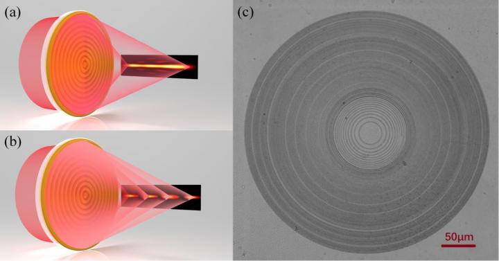
Credit: Opto-Electronic Advances
In a new publication from Opto-Electronic Advances; DOI https:/
Ultrathin and lightweight, metalenses are becoming increasingly significant for their use in photonic chips, biosensors and micro imaging systems such as smart phone cameras.
Compared to conventional lenses, metalenses can improve the image quality of current cameras, by enhancing resolution and removing spherical and chromatic aberrations. A single ultrathin (less than the thickness of 1/100 of a human hair) metalens element can be used instead of the multiple element imaging systems required by conventional lenses. Due to the unique light-matter interaction in a confined 2D plane, 2D materials are ideal for use with metalenses, further reducing the required thickness of the lens. 2D Graphene family materials, for example graphene oxides, are air-stable, have many applications and are low-cost and easy to fabricate in large scale. They remain stable in extreme environments, for example lower earth orbit in aerospace, so have potential use in satellites replacing the current bulky lenses and improving imaging quality and lowering launch costs.
The authors of this article developed 200 nm thick graphene oxide metalenses to generate specialized focal intensity distributions. The graphene oxide metalenses have the capability of controlling light amplitude (i.e., transparency of the lens) and phase (refractive index and thickness of the lens) simultaneously. This differs from other metalenses, which introduce the modulations through multi-step nanofabrication or multilevel of nano-elements, the modulations of graphene oxide lenses are locally introduced by the laser photo-reduction process, which converts graphene oxide to graphene material. During the reduction process, the material becomes thinner and has a higher refractive index and absorption. Based on the simultaneous phase and amplitude modulations, the authors demonstrate precise control of the focal intensity distributions by creating a super-resolved ultra-long optical needle and an axial multifocal array, which are extremely challenging for other metalenses.
Graphene oxide metalenses will find broad applications in integrated photonics and compact photonic systems, including microscopic imaging, optical manipulation and photonic chips, and can be integrated on microfluidic chips to form lab-on-a-chip biophotonic devices. This research forms a basis for the development of graphene-based ultrathin integratable photonic devices and paves the way for broader applications, such as replacing current cell phone camera lens potentially allowing a reduction in the thickness of current cell phones.
###
Article reference: Hongtao Wang, Chenglong Hao, Han Lin, Yongtian Wang, Tian Lan, Chengwei Qiu and Baohua Jia, Generation of super-resolved optical needle and multifocal array using graphene oxide metalenses, Opto-Electronic Advances, 2021, ISSN 2096-4579, https:/
Keywords: femtosecond laser reduction; graphene oxide; metalens; multifocal spots; optical needle
Led by Professor Baohua Jia, the Centre for Translational Atomaterials (CTAM) at Swinburne University of Technology, Victoria, Australia focuses on fundamental research of atomic material (atomaterials) design, engineering as well as the development of transformative technologies of such novel materials. With 70 research staff and students, CTAM is the world’s first dedicated centre for atomaterial research and translation. Current research areas include intelligent atomic structure design and synthesis, in-situ characterization, functional device design and fabrication, structure design and optimization as well as device engineering and translation.
Opto-Electronic Advances (OEA) is a high-quality, open access, peer reviewed research journal that is published by The Institute of Optics and Electronics, Chinese Academy of Sciences. OEA provides a platform for researchers, academicians, professionals, practitioners, and students to impart and share knowledge in the form of high quality empirical and theoretical research papers covering the topics of optics, photonics and optoelectronics.
Since its launch in March 2018, OEA has expanded into a monthly publication schedule. From 2020 OEA is indexed by Science Citation Index Expanded (SCIE) and SCOPUS. From the current Web of Science (WoS) data, OEA expects that the June 2021 Journal Citation Report (JCR) should show that the journal has an Impact Factor of about 10.
More information: http://www.
Editorial Board: http://www.
All issues available in the online archive (http://www.
Submissions to OEA may be made using ScholarOne (https:/
ISSN: 2096-4579
CN: 51-1781/TN
Contact Us: [email protected]
Twitter: @OptoElectronAdv
Media Contact
Morgan lyons
[email protected]
Related Journal Article
http://dx.


