WASHINGTON – The U.S. Naval Research Laboratory’s gallium nitride (GaN) wafers, also called large-area engineered substrates, can enable GaN to potentially be a displacement technology for silicon semiconductors used in microelectronics, particularly in power electronics.
A typical substrate in microelectronics is a thin semiconductor crystalline disk or wafer. An engineered substrate is a composite structure consisting of polycrystalline and crystalline layers that are optimized for a good thermal expansion and crystalline match to GaN. The excellent thermal expansion match permits thick GaN epitaxial layers which has enabled 1200 volts and beyond GaN power switches.
Karl Hobart and Francis “Fritz” Kub, both electrical engineers and heads of the High Power Devices Section and High Power Electronics Branch at the U.S. Naval Research Laboratory, are the lead inventors for GaN engineered substrates.
“What’s unique about GaN material is it’s a wide-bandgap semiconductor, so it can support higher electric fields,” Hobart said. “It is also a useful light emitter and a very fast switch for high frequency applications but we’re more interested in high voltage, high electric field devices.”
GaN operates at much higher voltages, frequencies and temperatures than conventional semiconductor material such as silicon, and enables more efficient, smaller, lighter, faster and lower cost end products.
The NRL Office of Technology Transfer led by Amanda Horansky-McKinney and her team fostered development and commercialization for this particular GaN technology. They were recognized in April with a 2021 Excellence in Technology Transfer Award from the Federal Laboratory Consortium.
Hobart and Kub came up with the basic research idea for these GaN substrates in the early 2000s.
“At that time, we recognized that the existing GaN substrate technology was neither scalable nor affordable. We envisioned a new ‘engineered’ substrate technology that could achieve large diameters consistent with advanced semiconductor manufacturing foundries,” Hobart said.
Through the efforts of NRL’s Office of Technology Transfer, GaN substrates have made their way through a series of companies each with differing angles on commercialization.
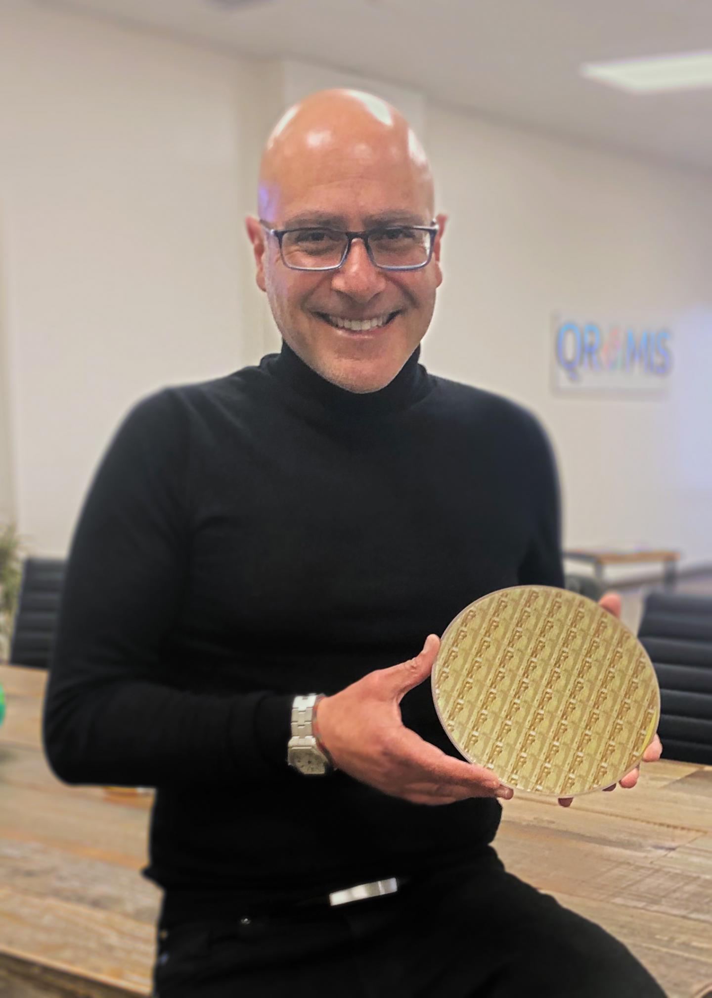
“The ultimate recipient of the transferred technology is silicon-valley based QROMIS, Inc.,” Horansky-McKinney said. “QROMIS has become well-positioned to do exactly what we hope our licensees will do – invest and develop an intellectual property base supporting a competitive market position for their products, using NRL technology as the base.”
Cem Basceri, CEO and president of QROMIS, said working with NRL has been an extremely positive experience and the partnership and team work exceeded his expectations.
“In terms of quality of work, especially NRL’s Tech Transfer, Ms. Horansky-McKinney did a great job and helped making everything go so smoothly,” Basceri said. “Teaming up with NRL’s scientists and engineers is excellent, because they have very unique and innovative ideas which can turn into commercial solutions.”
The technology transfer partnership was initiated in 2009 when six patents formed the basis of NRL’s innovation and then licensed to a small business named Amberwave Systems Corporation. The company was then acquired by Micron Technology, which invested in developing the GaN substrate concept further under the NRL license.
“It was encouraging that our innovation was recognized by industry as the future of GaN technology and they were dedicated to further development toward commercialization,” Kub said. “We thought our technology was a good idea, but they must have thought it was a great idea to make such a large investment in the technology.”
Historically, there have been shortcomings with GaN wafers such as the thermal expansion mismatch between silicon. However, NRL’s research experts and their commercial partners were able to solve the issue by creating a thin inexpensive wafer made out of polycrystalline aluminum nitride, which has a close thermal expansion match to gallium nitride. Additionally, a thin layer of single crystal silicon was added for GaN nucleation and to avoid any mechanical issues. They are now able to produce a wafer with optimal component performance and affordability.
QROMIS took these solutions to launch their commercial products, called QST® substrates and GaN-on-QST® epi wafers.
Hobart and Kub’s advice for other defense researchers working to transition their basic science and technology efforts from inception to commercialization: work closely with a company that’s interested in the technology.
“The partnerships between industry and NRL have contributed to a successful development and transfer of the technology that will greatly benefit the Navy and Marine Corps,” Horansky-McKinney said.
###
The U.S. Naval Research Laboratory Technology Transfer Office facilitates and promotes NRL’s innovative technologies in products and services to benefit the public and the Nation’s service men and women. Learn how NRL technologies are commercialized or how businesses can benefit from collaboration with some of the world’s most respected scientists at https:/
About the U.S. Naval Research Laboratory
NRL is a scientific and engineering command dedicated to research that drives innovative advances for the U.S. Navy and Marine Corps from the seafloor to space and in the information domain. NRL is located in Washington, D.C. with major field sites in Stennis Space Center, Mississippi; Key West, Florida; Monterey, California, and employs approximately 2,500 civilian scientists, engineers and support personnel.
For more information, contact NRL Corporate Communications at (202) 480-3746 or [email protected].
Media Contact
J. Raynel Koch
[email protected]
Original Source
https:/


