Credit: HKUST
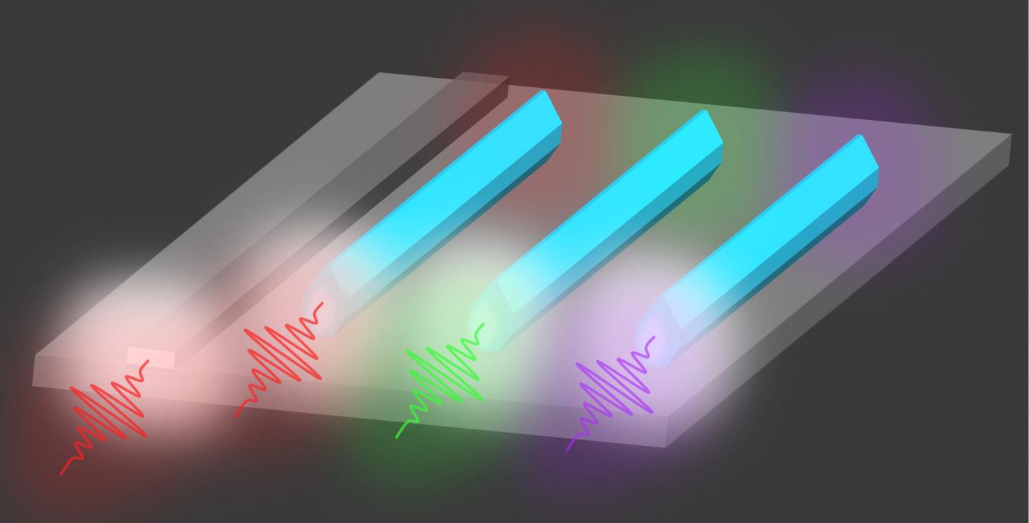
Researchers from the Hong Kong University of Science and Technology (HKUST) have reported the world’s first 1.5 μm III-V lasers directly grown on the industry-standard 220 nm SOI (silicon-on-insulators) wafers without buffer, potentially paving an opening to the “holy grail” for present silicon (Si-) photonics research.
Seamlessly bridging the active III-V light sources with the passive Si-based photonic devices, the demonstration could be deployed as light sources in integrated circuits to greatly improve circuit speed, power efficiency and cost-effectiveness.
In other conventional approaches of integrating III-V lasers on Si in the literature, thick III-V buffers up to a few micrometers are used to reduce the defect densities, which posts huge challenges for efficient light interfacing between the epitaxial III-V lasers and the Si-based waveguides.
For the first time in history, the research team led by Prof. LAU Kei-May of HKUST’s Department of Electronic and Computer Engineering and Post-doctoral Fellow Dr. HAN Yu devised a novel growth scheme to eliminate the requirement of thick III-V buffers and thus promoted efficient light coupling into the Si-waveguides. The bufferless feature points to a fully integrated Si-based photonic integrated circuits.
That has enabled the first demonstration of 1.5 μm III-V lasers directly grown on the industry-standard 220 nm SOI wafers using metal organic chemical vapor deposition (MOCVD). Previous demonstrations required non-industry-standard bulk Si or thick SOI wafers.
The research findings were recently published online in Optica in February 2020.
The world’s growing appetite for Internet services and the digitization of our lives leads to a vast amount of digital data being generated, processed, stored, and transmitted.
Silicon is the most widely used material in the manufacturing of semiconductors, which are embedded into nearly every piece of communications technology that we rely on every day, from computers and smartphones to datacenters and satellite communications.
But improvements in efficiency of conventional electronic data systems cannot catch up with the soaring data traffic, which calls for the integration of photonic functionalities onto the conventional Si-based electronic platform. The integration could produce optoelectronic integrated circuits with unparalleled speed and functionalities, and enable new applications.
Yet fundamental differences between Si and III-V materials means it is extremely challenging to directly grow III-V functionalities on the Si-platform.
Prof. Lau’s group at HKUST’s Phonics Technology Center has endeavored to integrate III-V materials and functionalities on mainstream silicon wafers for over a decade, innovating and optimizing various approaches to improve the performance of III-V lasers grown on Si, with the goal of progressively approach the requirements of the industry. This work is part of their project on monolithic integration of III-V lasers on silicon.
Their method saw them first devising a unique growth scheme to directly grow high quality III-V materials on the industry-standard 220 SOI platforms. Then, they characterized and evidenced the excellent crystalline quality of these epitaxial III-V materials through extensive transmission electron microscopy and photoluminescence measurements. The team designed and fabricated the air-cladded laser cavities based on numerical simulations and they eventually tested the devices which showed that the lasers could sustain room-temperature and low-threshold lasing in the technologically important 1.5 μm band under optical excitation.
The demonstration leads to the possibility and potential to monolithically integrate III-V lasers on the industry-standard 220 nm SOI wafers in an economical, compact, and scalable way.
Prof. Lau said: “If practically applied, our technology could enable a significant improvement of the speed, power consumption, cost-effectiveness, and functionality of current Si-based integrated circuits. Our daily electronic devices, such as smartphones, laptops and TVs – basically everything connected to the internet – will be much faster, cheaper, using much less power and multi-functional.”
Dr. Han added: “The next step of our research will be to design and demonstrate the first electrically-driven 1.5 μm III-V lasers directly grown on the 220 nm SOI platforms, and devise a scheme to efficiently couple light from the III-V lasers into Si-waveguides and thereby conceptually demonstrate fully-integrated Si-photonics circuits.”
###
Media Contact
Johnny Tam
[email protected]
852-235-88556
Related Journal Article
http://dx.


