In a significant advancement for imaging technology, researchers from ETH Zurich and Empa have developed a groundbreaking perovskite-based image sensor that promises to revolutionize photographic quality while operating efficiently in low-light environments. This innovation could redefine the capabilities of digital cameras, smartphones, and various fields requiring precise imaging, such as medical diagnostics and environmental monitoring. The novel sensor leverages lead halide perovskite, a semiconductor material that has gained attention for its unique properties, including high light sensitivity and customizable absorption characteristics, which allow for unprecedented imaging accuracy.
Traditionally, silicon-based sensors have dominated the image sensor market. While silicon effectively absorbs light across the visible spectrum, it utilizes filters to manage the color interpretation through its pixel structure. This pixelation strategy results in significant light loss as each pixel predominantly captures only one color—red, green, or blue—due to the necessity of filtering. Such dependency on filters not only wastes incoming light but also introduces artifacts and compromises image quality. The researchers’ shift toward perovskite technology aims to transcend these limitations, maximizing light capture and color accuracy without the need for bulky filters.
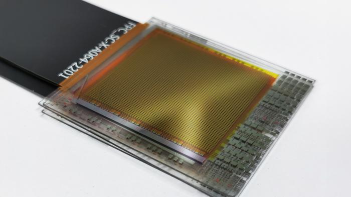
The core innovation of these perovskite sensors stems from the unique ability to stack the color-detecting layers vertically instead of aligning them side-by-side, as is standard with silicon sensors. Each pixel in a perovskite sensor can be engineered to absorb light at specific wavelengths—red, green, or blue—based solely on its chemical composition. Adding varying amounts of iodine, bromine, or chlorine fine-tunes the light absorption for different colors. This configuration allows each pixel to absorb all the available light while remaining transparent to other wavelengths, representing a radical shift from conventional image sensing.
.adsslot_DgzLcaxt2q{ width:728px !important; height:90px !important; }
@media (max-width:1199px) { .adsslot_DgzLcaxt2q{ width:468px !important; height:60px !important; } }
@media (max-width:767px) { .adsslot_DgzLcaxt2q{ width:320px !important; height:50px !important; } }
ADVERTISEMENT
The implications of this innovative stacking technology are vast. In theory, these perovskite sensors can capture up to three times more light and provide corresponding increases in spatial resolution compared to traditional sensors of comparable size. Researchers from Kovalenko’s team have previously demonstrated the effectiveness of this technology using oversized individual pixels made from large single crystals. The recent development of two fully functional thin-film prototypes marks a significant evolution from concept to practical application, showcasing that perovskite-based image sensors can be miniaturized effectively for real-world use.
This newfound capacity for miniaturization is vital not only for consumer electronics but also for fields needing specific imaging solutions. In environments like agriculture, hyperspectral imaging—where sensors detect several wavelengths beyond standard RGB channels—is highly advantageous. Perovskite technologies facilitate the design of image sensors that can identify specific colors, improving monitoring and analysis processes in agriculture and environmental science. Traditional silicon sensors struggle with such demands due to their narrow color bandwidths and resultant optical imprecision.
Moreover, the researchers emphasize the versatility of perovskite sensors in medical applications, where precision imaging can significantly impact diagnostics and treatment monitoring. The ability to define various optimal wavelength ranges for absorption opens doors for using these sensors in advanced medical imaging techniques, offering much more than the simplistic RGB filter approach. This transition could lead to breakthroughs in areas such as drug detection, cellular imaging, and tissue analysis.
While the prototypes have demonstrated commendable success, the team is focused on further refining the technology. Current pixel sizes range between 0.5 and 1 millimeter, which is significantly larger than typical micrometer-scale pixels found in commercial sensors. The research team believes it’s possible to shrink perovskite pixels even further than silicon counterparts, presenting compelling evidence for the future applicability of this technology. To achieve advancements in size and efficiency, the electronic connections and processing methodologies need optimization to suit the unique characteristics of perovskite rather than traditional silicon.
Optimizing readout electronics for perovskite technology presents another layer of challenges, yet the research team remains optimistic. The properties of perovskite as a semiconductor differ markedly from silicon, necessitating new approaches to electronic circuitry and signal processing. However, researchers are confident that overcoming these obstacles will be critical to niche areas that may make substantial advancements thanks to innovative image sensing technologies.
In summary, the emergence of perovskite-based image sensors signifies a major leap forward in imaging technology, offering enhanced light sensitivity, minimized artifacts, and elevated resolution without the need for traditional filtering methods. As the researchers continue to refine their prototypes and work toward miniaturization, the future holds exciting possibilities across numerous disciplines. The potential applications of this technology extend beyond the consumer market into vital sectors such as healthcare and environmental monitoring, where precision is paramount, ultimately promising a new era of imaging excellence.
Subject of Research: Development of perovskite-based image sensors
Article Title: Vertically stacked monolithic perovskite colour photodetectors
News Publication Date: 18-Jun-2025
Web References: DOI Link
References: Nature Journal publication
Image Credits: Empa / ETH Zurich
Keywords
Perovskite, image sensor, light sensitivity, digital imaging, semiconductor, hyperspectral imaging, medical diagnostics, environmental monitoring, color accuracy, miniaturization, receptor technology, photographic quality.
Tags: advantages of perovskite over siliconbreakthrough in photographic qualitycustomizable absorption characteristicsdigital camera innovationenvironmental monitoring sensorshigh light sensitivity sensorsImaging technology advancementslow-light photography solutionsmedical diagnostics imaging technologyperovskite-based image sensorreducing light loss in imagingsemiconductor materials in imaging


