In a groundbreaking development poised to transform the semiconductor industry, researchers at Cornell University have unveiled a novel high-resolution 3D imaging technique capable of identifying atomic-scale defects within computer chips for the very first time. This remarkable advancement, realized through a collaboration involving Taiwan Semiconductor Manufacturing Company (TSMC) and Advanced Semiconductor Materials (ASM), promises to impact the vast array of modern electronics — spanning from smartphones and automobiles to sophisticated AI data centers and the frontier technology of quantum computing.
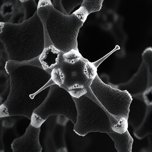
The cornerstone of this achievement lies in utilizing electron ptychography, a sophisticated computational imaging method. This technique employs an electron microscope pixel array detector (EMPAD), a cutting-edge technology co-developed by the Muller research group at Cornell, to capture intricate electron scattering patterns as electrons traverse transistor channels. By comparing subtle variations in these scattering patterns across different scan positions, the method reconstructs images of unparalleled clarity, capable of resolving individual atoms with extraordinary precision. Such resolution not only marks a significant leap beyond traditional imaging but also earns recognition from the Guinness World Records for the highest resolution microscopy images ever recorded.
At the heart of every modern computer chip lies the transistor — a minuscule electronic switch that controls current flow through a nanoscale channel, governed by an electric gate. As semiconductor manufacturing has pushed components to ever-smaller dimensions, transistor channels have constricted to widths on the order of 15 to 18 atoms. While this shrinkage enables remarkable computational power and efficiency, it poses a daunting challenge: even the slightest irregularities or defects at the atomic level in these channels can severely impair transistor performance, acting as bottlenecks or sources of leakage current.
David Muller, the Samuel B. Eckert Professor of Engineering and leader of the project, reflects on this evolution using an apt analogy: “The transistor is like a tiny pipe for electrons. If the pipe walls are rough, they hinder the flow. Now, measuring and distinguishing good walls from bad ones on the atomic scale is critical.” Traditional imaging methods lacked the necessary spatial resolution to probe these defects directly, relegating engineers to indirect inference and guesswork.
The research journey traces back to Muller’s pioneering work in semiconductor materials during his tenure at Bell Labs in the late 1990s and early 2000s. There, he and colleague Glen Wilk worked on overcoming the limitations of silicon dioxide, the conventional gate dielectric material that leaked excessive current at nanoscale dimensions. Their exploration led to the adoption of hafnium oxide, a breakthrough gate material that swiftly became the industry standard, enabling transistors to scale down while retaining control and efficiency. The latest imaging innovation stands as a natural extension of this previous work, harnessing modern electron microscopy advancements to explore transistor interiors with clarity reminiscent of upgrading from rudimentary biplanes to cutting-edge jets.
Central to this imaging technique is the EMPAD detector, which collects comprehensive electron diffraction data without sacrificing speed or sensitivity. By combining this hardware with sophisticated computational algorithms in electron ptychography, the research team achieves reconstructions that surpass diffraction and lens aberration limits typical of conventional electron microscopes. This capability enables an unprecedented atomic-level characterization of transistor channel interfaces, surface roughness, and defect populations — phenomena previously relegated to estimation rather than direct observation.
Applying this method to test structures grown at the nanoelectronics research hub Imec, the researchers uncovered previously invisible interface irregularities dubbed “mouse bites.” These tiny defects are the result of cumulative imperfections introduced during the hundreds or thousands of manufacturing steps such as chemical etching, material deposition, and thermal treatments. Each processing stage subtly impacts the atomic landscape, and until now, engineers lacked a direct means to visualize how these steps affect transistor channel roughness and atomic arrangement.
The implications of this capability are transformative. The ability to directly observe atomic defects enables semiconductor engineers to debug fabrication processes with unprecedented granularity, optimizing each step to minimize deleterious effects on device performance. This is especially critical as transistor architectures continue evolving toward complex three-dimensional configurations — compact “apartment-block”-style stacks that replace sprawling two-dimensional layouts, pushing dimensions below the scale of viruses or even molecules inside cells.
Moreover, this imaging methodology holds promise beyond classical silicon electronics. Emerging quantum computing platforms demand immaculate atomic arrangements and interface qualities to preserve fragile quantum states. The electron ptychography technique affords scientists an invaluable tool to probe and understand the structural intricacies that govern device reliability and quantum coherence, a frontier yet to be fully mastered.
Shake Karapetyan, the study’s lead author and a doctoral student at Cornell, emphasizes the broader scientific and technological horizons unlocked by this tool. “Now, we can track every atom, diagnose where defects form, and gain engineering control previously unattainable. This opens avenues not only for silicon chips but for next-generation materials and devices where atomic precision is paramount.”
Co-directed by Muller, the Kavli Institute at Cornell for Nanoscale Science alongside the Cornell Center for Materials Research (CCMR) provided critical support for the microscopy facilities, with additional funding from the National Science Foundation’s Platform for the Accelerated Realization, Analysis and Discovery of Interface Materials (PARADIM). The research receives corporate backing from TSMC, whose engineers contributed key expertise in semiconductor manufacturing and analysis.
This landmark study, published on February 23 in Nature Communications, represents a pinnacle in the convergence of materials science, computational physics, and electronic engineering — a testament to the power of interdisciplinary collaboration in solving challenges at the atomic frontier. As the semiconductor landscape races toward smaller, faster, and more energy-efficient devices, the ability to visualize the very building blocks of transistor operation promises to accelerate innovation and usher in a new era of chip debugging, development, and design.
Subject of Research: Semiconductor transistor atomic-scale defects
Article Title: Atomic-Scale Imaging of Semiconductor Transistor Defects via Electron Ptychography
News Publication Date: February 23, 2026
Web References:
Nature Communications article DOI: 10.1038/s41467-026-69733-1
Kavli Institute at Cornell for Nanoscale Science: https://www.kicnano.cornell.edu/
Cornell Center for Materials Research (CCMR): https://www.ccmr.cornell.edu/
PARADIM: https://www.paradim.org/
Guinness World Records for highest resolution microscope: http://www.guinnessworldrecords.com/world-records/highest-resolution-microscope
References:
Karapetyan, S., Muller, D. A., Zeltmann, S., Chen, T.-K., Hou, V., et al. (2026). Direct imaging of atomic-scale defects in semiconductor transistors using electron ptychography. Nature Communications, DOI:10.1038/s41467-026-69733-1.
Image Credits: Cornell University research group and collaborators
Tags: advanced electron scattering techniquesAI data center hardware defectsatomic-scale defects in semiconductorsCornell University semiconductor researchelectron ptychography imagingEMPAD technology in chip analysisGuinness World Record microscopy imageshigh-resolution 3D electron microscopyquantum computing chip inspectionsemiconductor manufacturing quality controlsemiconductor transistor defect detectionTSMC semiconductor collaboration

