Credit: University of Texas at Dallas/Qingxiao Wang and Moon Kim
WEST LAFAYETTE, Ind. — Computer chips use billions of tiny switches, called transistors, to process information. The more transistors on a chip, the faster the computer.
A material shaped like a one-dimensional DNA helix might further push the limits on a transistor’s size. The material comes from a rare earth element called tellurium.
Researchers found that the material, encapsulated in a nanotube made of boron nitride, helps build a field-effect transistor with a diameter of two nanometers. Transistors on the market are made of bulkier silicon and range between 10 and 20 nanometers in scale.
The research is published in the journal Nature Electronics. Engineers at Purdue University performed the work in collaboration with Michigan Technological University, Washington University in St. Louis, and the University of Texas at Dallas.
Over the past few years, transistors have been built as small as a few nanometers in lab settings. The goal is to build transistors the size of atoms.
Peide Ye’s lab at Purdue is one of many research groups seeking to exploit materials much thinner than silicon to achieve both smaller and higher-performing transistors.
“This tellurium material is really unique. It builds a functional transistor with the potential to be the smallest in the world,” said Ye, Purdue’s Richard J. and Mary Jo Schwartz Professor of Electrical and Computer Engineering.
In 2018, the same research team at Purdue discovered tellurene, a two-dimensional material derived from tellurium. They found that transistors made with this material could carry significantly more electrical current, making them more efficient.
The discovery made them curious about what else tellurium could do for transistors. The element’s ability to take the form of an ultrathin material in one dimension could help with downsizing transistors even further.
One way to shrink field-effect transistors, the kind found in most electronic devices, is to build the gates that surround thinner nanowires. These nanowires are protected within nanotubes.
Jing-Kai Qin and Pai-Ying Liao, Purdue electrical and computer engineering doctoral students, led work in figuring out how to make tellurium as small as a single atomic chain and then build transistors with these atomic chains or ultrathin nanowires.
They started off growing one-dimensional chains of tellurium atoms. Wenzhuo Wu’s lab at Purdue synthesized bare tellurium nanowires for comparison. A team led by Li Yang at Washington University simulated how tellurium might behave.
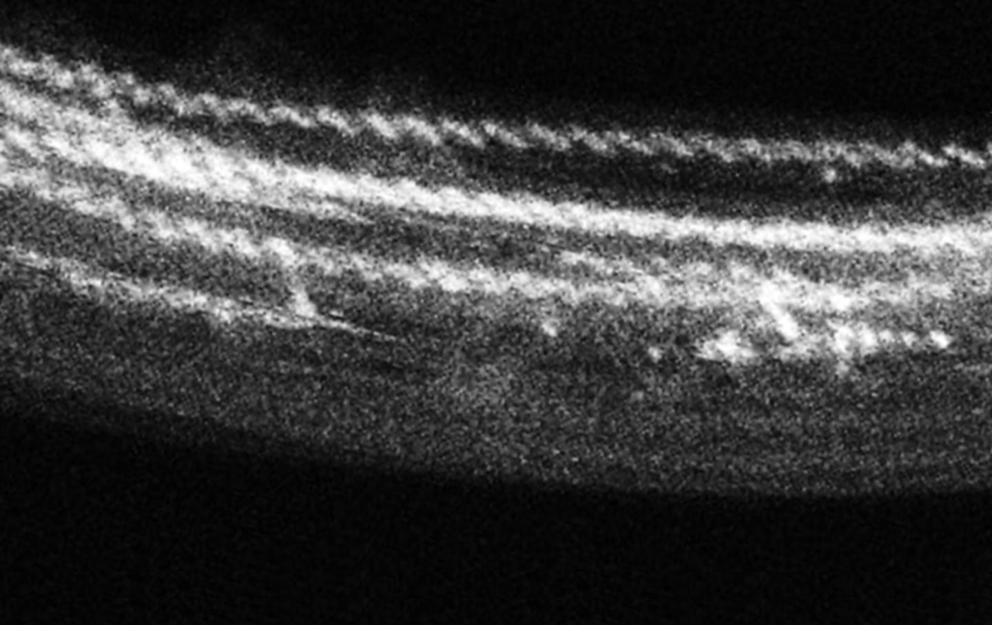
The researchers were surprised to find that the atoms in these one-dimensional chains wiggle. These wiggles were made visible through TEM imaging performed by Moon Kim at the University of Texas at Dallas and Hai-Yan Wang at Purdue.
“Silicon atoms look straight, but these tellurium atoms are like a snake. This is a very original kind of structure,” Ye said.
The wiggles were the atoms strongly bonding to each other in pairs to form DNA-like helical chains, then stacking through weak forces called van der Waals interactions to form a tellurium crystal.
These van der Waals interactions would set apart tellurium as a more effective material for single atomic chains or one-dimensional nanowires compared with others because it’s easier to fit into a nanotube, Ye said.
Since the opening of a nanotube can’t be any smaller than the size of an atom, tellurium helices of atoms could achieve smaller nanowires and, therefore, smaller transistors.
The researchers built a transistor with a tellurium nanowire encapsulated in a boron nitride nanotube, provided by physics professor Yoke Khin Yap’s lab at the Michigan Technological University. A high-quality boron nitride nanotube effectively insulates tellurium, making it possible to build a transistor.
Xianfan Xu’s lab at Purdue characterized the material’s properties with Raman spectroscopy to benchmark its performance.
“This research reveals more about a promising material that could achieve faster computing with very low power consumption using these tiny transistors,” said Joe Qiu, program manager for the U.S. Army Research Office, which funded this work. “That technology would have important applications for the Army.”
###
The work was also partly funded by the National Science Foundation, Air Force Office of Scientific Research, and the Defense Advanced Research Projects Agency. The researchers conducted experiments in Purdue Discovery Park’s Birck Nanotechnology Center.
About Discovery Park
Discovery Park is a place where Purdue researchers move beyond traditional boundaries, collaborating across disciplines and with policymakers and business leaders to create solutions for a better world. Grand challenges of global health, global conflict and security, and those that lie at the nexus of sustainable energy, world food supply, water and the environment are the focus of researchers in Discovery Park. The translation of discovery to impact is integrated into the fabric of Discovery Park through entrepreneurship programs and partnerships.
ABSTRACT
Raman response and transport properties of tellurium atomic chains encapsulated in nanotubes
Jing-Kai Qin1, Pai-Ying Liao1, Mengwei Si1, Shiyuan Gao3, Gang Qiu1, Jie Jian1, Qingxiao Wang4, Si-Qi Zhang2, Shouyuan Huang3, Adam Charnas1, Yixiu Wang1, Moon J. Kim4, Wenzhuo Wu1, Xianfan Xu1, Hai-Yan Wang1, Li Yang3, Yoke Khin Yap2, Peide D. Ye1
1Purdue University, West Lafayette, IN, USA
2Michigan Technological University, Houghton, MI, USA
3Washington University in St. Louis, St. Louis, MO, USA
4University of Texas at Dallas, Richardson, TX, USA
DOI: 10.1038/s41928-020-0365-4
As a unique elemental one-dimensional (1D) van der Waals (vdW) material, ultra-narrow tellurium nanowires (Te NWs) at the few-chain limit are expected to exhibit intriguing physical properties which are remarkably different from those in bulk form. In this work, we successfully isolate few-chain and even single-chain 1D vdW Te NWs by carbon nanotube (CNT) or boron nitride nanotube (BNNT) encapsulation. The number of Te atomic chains was controlled by the inner diameter (ID) of the nanotubes. The Raman response suggests the interaction between a single-atomic Te chain with a CNT is weak and the inter-chain interaction between Te becomes stronger as the number of chains increases. By the encapsulation of a BNNT, 1D vdW Te NW enables a large current density even with a few atomic chains. Compared with SiO2 supported bare Te NWs, the ampacity of Te NWs grown inside BNNTs can be dramatically enhanced with a high current density of 1.5×10⁸ A cm-2, exceeding that of most semiconducting materials. Te NW field-effect transistors (FETs) were also successfully demonstrated with the smallest diameter of 2 nm.
Media Contact
Kayla Wiles
[email protected]
765-494-2432
Original Source
https:/
Related Journal Article
http://dx.


