A groundbreaking leap in semiconductor technology promises to revolutionize the landscape of electronic devices, promising cleaner energy, stronger cellular signals, and more precise sensors across industries. Researchers at the University of Michigan, led by the distinguished engineering professor Zetian Mi, have uncovered a remarkably simple yet profoundly effective thermal annealing process that amplifies the piezoelectric properties of scandium aluminum nitride (ScAlN) films by an unprecedented factor of eight. This advancement has far-reaching implications for the next generation of microelectronics and photonics, potentially reshaping applications from everyday consumer devices to critical aerospace technologies.
Piezoelectric materials, which generate electrical charge in response to mechanical stress, serve as pivotal components in an array of modern technologies that touch daily life. Their prevalence spans from the cluttered interiors of cell phones, where they act as precise filters to suppress signal noise, to automotive safety systems that rely on their rapid sensor response to trigger airbags and monitor tire integrity. Enhancing the piezoelectric effect in these materials translates directly into improvements in sensitivity, efficiency, and durability, fundamentally improving the performance of countless devices that rely on these phenomena.
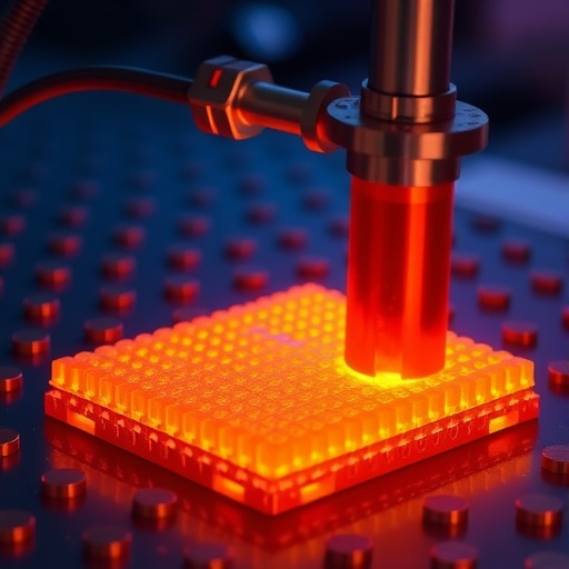
The team’s innovative approach involves subjecting scandium aluminum nitride thin films to a meticulously controlled annealing process—heating the material to 700 degrees Celsius for a full two hours within a specialized chamber. This thermal treatment fosters critical atomic rearrangements within the thin crystal layers, correcting structural defects that typically impede their piezoelectric response. The result is an extraordinary eight-fold increase in piezoelectricity compared to the properties seen in commercially available materials, effectively pushing the envelope toward new possibilities in device engineering.
Central to this enhancement is the reorientation of microscopic structural “grains” within the material. These grains, initially misaligned during the film’s growth phase, contribute unevenly to the piezoelectric effect due to their directional sensitivity. The annealing process supplies sufficient thermal energy to coax these grains into better alignment with the material’s overall crystalline axis. This realignment maximizes their collective contribution, substantially magnifying the measurable piezoelectric response and thereby enhancing sensor performance and energy conversion efficiencies.
The implications of such a leap are manifold and expansive. Enhanced piezoelectric films crafted through this simple yet effective step could lead to the creation of ultrasensitive pressure and vibration sensors crucial for monitoring structural health in aerospace engineering or advanced medical ultrasound imaging. Moreover, their application extends into smart city infrastructure, where energy-harvesting traffic lights powered by the vibrations of passing trucks could become a reality, promoting sustainable urban energy solutions.
Remarkably, the annealing process devised by the researchers aligns closely with existing industrial fabrication standards, meaning the pathway to commercial adoption is streamlined. Industry players stand to upgrade their semiconductor components dramatically without incurring substantial additional manufacturing costs or overhauling established workflows. This seamless integration amplifies the innovation’s appeal, promising rapid deployment of more capable piezoelectric devices in both commercial and defense sectors.
Funding for this trailblazing research comes from the Defense Advanced Research Projects Agency (DARPA) as part of a collaborative project involving the University of Florida, the University of Michigan College of Engineering, and the Army Research Office. This partnership aims to leverage improved piezoelectric materials for creating next-generation atomic clocks with hyper-precision synchronization capabilities, which hold critical importance for national defense and communication systems.
The multi-institutional nature of the work further enhances the rigor and applicability of the findings. Contributions from researchers at the University of Florida and Pennsylvania State University encompassed interdisciplinary expertise that enriched the study’s scope and depth, ensuring robustness in both theoretical insight and experimental verification. The well-equipped Lurie Nanofabrication Facility and the Michigan Center for Materials Characterization provided essential infrastructure for processing and evaluating the advanced films.
Intellectual property considerations are already being addressed, with patent applications underway and active pursuits of industrial partnerships through the University of Michigan’s Innovation Partnerships program. This strategy indicates clear intent to move beyond academia and realize tangible commercial impacts, accelerating the translation of this technology from lab bench to market-ready devices.
Professor Zetian Mi, whose credentials also include appointments in electrical and computer engineering and materials science and engineering, leads these transformative efforts. His vision integrates materials science innovation with practical engineering solutions that promise broad societal benefit. The comprehensive study detailing the enhancement mechanisms and material characterizations has been published in Nature Communications, providing open insight into the scientific community to foster further advances.
This breakthrough shines a spotlight on the latent potential locked within well-studied semiconductor materials and underscores how revisiting fabrication processes with fresh perspectives can yield exponential improvements. The engineering simplicity paired with profound functional gains serves as a potent reminder that innovation transcends complexity, and even incremental process tweaks can redefine the technological landscape.
As the scientific and industrial communities continue to digest and build upon these findings, the future of piezoelectric devices looks brighter than ever. From empowering smarter energy harvesting and ultra-precise sensing to enabling new frontiers in medical and defense technologies, this enhancement in scandium aluminum nitride films epitomizes the transformative power of marrying material science with innovative fabrication techniques.
Subject of Research: Enhancement of piezoelectric properties in semiconductor materials via thermal annealing
Article Title: Unprecedented enhancement of piezoelectricity of wurtzite nitride semiconductors via thermal annealing
Web References:
Study DOI: https://doi.org/10.1038/s41467-025-59179-2
University of Michigan Engineering: https://mi.engin.umich.edu/
Lurie Nanofabrication Facility: https://lnf.umich.edu/
Michigan Center for Materials Characterization: https://mc2.engin.umich.edu/
References:
Mi, Z., Mondal, S., Tanim, M. M. H., et al. (2024). Unprecedented enhancement of piezoelectricity of wurtzite nitride semiconductors via thermal annealing. Nature Communications. DOI: 10.1038/s41467-025-59179-2
Keywords
Piezoelectricity, Scandium Aluminum Nitride, Semiconductor Materials, Thermal Annealing, Microelectronics, Photonics, Materials Engineering, Electrical Engineering, Materials Science, Condensed Matter Physics
Tags: aerospace technology innovationsautomotive safety systems and sensorsconsumer electronics improvementselectrical charge generation materialsenergy-efficient electronic devicesimproved sensor efficiencymechanical stress response materialsmicroelectronics and photonics applicationspiezoelectric properties enhancementscandium aluminum nitride filmssemiconductor technology advancementsthermal annealing process


