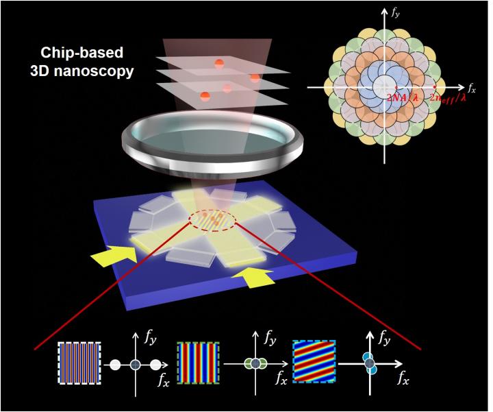
A chip-compatible 3D nanoscopy answers

Credit: ©Science China Press
Compared with the superresolution microscopy that bases on squeezing the point spread function in the spatial domain, the superresolution microscopy that broadens the detection range in the spatial frequency domain through the spatial-frequency-shift (SFS) effect shows intriguing advantages including large field of view, high speed, and good modularity, owing to its wide-field picture acquisition process and universal implementation without using special fluorophores labeling.
To enable spatial-frequency-shift microscopy with a superresolution at the subwavelength scale, it is essential to use the near-field evanescent wave with a larger wave vector than the far-field propagation wave for illumination, which can be built on the integrated photonics, paving the way for compact nanoscopy on a thin chip. In recent years, the research group led by Dr. Xu Liu and Dr. Qing Yang from Zhejiang University pioneered in using the evanescent wave illumination with large wave vector and long propagation distance for superresolution imaging, and achieved the chip-based label-free spatial-frequency-shift superresolution microscopy with a field of view 1-2 magnitude larger than the other wide-field label-free superresolution techniques.
However, the lack of an approach to actively tune the spatial-frequency-shift in a large range hampers the progress to achieve deep-subwavelength resolution through evanescent illumination with ultra-large wave vectors. When the wave vector of the illumination surpasses two folds of the cutoff frequency of the objective, a missing band exists between the shifted components and the zeroth component in the spatial frequency domain, which causes severe artifacts and distortion in the image. It thus restricts the resolution below triple of the Abbe diffraction limit of the detection system, as shown in Fig. 1.
In this month’s cover article in the Journal of SCIENCE CHINA Physics, Mechanics & Astronomy, the researchers propose a broadly-tunable large-spatial-frequency-shift effect and a chip-compatible 3D nanoscopy. With their method, the resolution of the linear optical system can be freely improved using an illumination chip of a larger effective refractive index without a theoretical limit. This method is also significant complementation to the Nobel-prize-awarded superresolution techniques that rely on labeling sample with fluorophores of nonlinear property and requires a point-by-point scanning process or capturing thousands of raw images. Simultaneously, compared to traditional superresolution microscopy imaging technology, this method is based on on-chip waveguide illumination and has the advantages of integration, low cost, and high stability. It can be further integrated with microfluidic and optoelectronic functional chips, providing a comprehensive research platform for the study of modern biological problems.
Dr. Qing Yang, one of the corresponding authors, introduced, “In order to avoid the missing band in the large -spatial-frequency-shift microscopy and achieve the deep-subwavelength resolution, we proposed the method of tunable large-spatial-frequency-shift microscopy and proposed several approaches to actively tune the spatial-frequency-shift value. In the early days, we use multiple-wavelength illumination to tune the spatial-frequency-shift value, while its tuning range is very limited. We must find other ways that allow the spatial-frequency-shift value to be tuned much more broadly.”
This research reports a wide-range 3D tunable deep SFS imaging method compatible with photonic chips, which makes the resolution enhancement of SFS imaging fundamentally get rid of the limitation of the detection aperture and no longer has the theoretical limit. In the lateral dimension, the spatial-frequency-shift tunability is realized by modulating the azimuthal propagation direction of two evanescent waves. The effective wave vector of their superposition can be tuned actively and broadly to enable a wide-range and complete detection in the spatial frequency domain, as shown in Fig. 2. In the vertical dimension, a sectional saturation effect by intensity modulation is used to tune the vertical spatial frequency spectrum of the evanescent illumination so as to solve the vertical spatial distribution within the evanescent penetration depth. Finally, a 3D superresolution image can be achieved by multiplying the lateral and vertical distribution together.
The researchers select GaP as the waveguide material, considering its high refractive index and low optical loss in the visible spectrum. A lateral resolution of ?/9, which is five folds of the diffraction-limited resolution, and a vertical localization precision of Dr. Xu Liu introduced, “This proposed 3D large-spatial-frequency-shift tuning method is compatible with waveguides chip and can provide a mass-producible and robust chip module endowing a standard microscope with fast, large FOV and 3D deep-subwavelength resolving capability. With the improvement of micro-nano processing technology and the establishment of photonic integrated chip production lines, on-chip integrated photonic chips can reduce costs and achieve mass production, which would put forward the real application of deep-subwavelength superresolution in biomedicine, life science, and materials, etc.”
###
This research was funded by the National Natural Science Foundation of China (Grant Nos. 61735017, 61822510, 62020106002, 61905097, and 62005250), the Zhejiang Provincial Natural Science of China (Grant No. LR17F050002), and the Zhejiang University Education Foundation Global Partnership Fund.
See the article:
Xiaowei Liu, Mingwei Tang, Chao Meng, Chenlei Pang, Cuifang Kuang, Wei Chen, Clemens F. Kaminski, Qing Yang, and Xu Liu, Chip-compatible wide-field 3D nanoscopy through tunable spatial frequency shift effect, SCIENCE CHINA Physics, Mechanics & Astronomy, 2021, 9 (294211).
https:/
Media Contact
Yan Bei
[email protected]
Related Journal Article
http://dx.


