Metalenses, nano-artificial structures capable of manipulating light, offer a technology that can significantly reduce the size and thickness of traditional optical components. Particularly effective in the near-infrared region, this technology holds great promise for various applications such as LiDAR which is called the ‘eyes of the self-driving car’, miniature drones, and blood vessel detectors. Despite its potential, the current technology requires tens of millions of won even for fabricating a metalens the size of a fingernail, posing a challenge for commercialization. Fortunately, a recent breakthrough shows promise of reducing its production cost by one thousandth of the price.
Credit: POSTECH
Metalenses, nano-artificial structures capable of manipulating light, offer a technology that can significantly reduce the size and thickness of traditional optical components. Particularly effective in the near-infrared region, this technology holds great promise for various applications such as LiDAR which is called the ‘eyes of the self-driving car’, miniature drones, and blood vessel detectors. Despite its potential, the current technology requires tens of millions of won even for fabricating a metalens the size of a fingernail, posing a challenge for commercialization. Fortunately, a recent breakthrough shows promise of reducing its production cost by one thousandth of the price.
A collaborative research team (POSCO-POSTECH-RIST Convergence Research Team), comprising Professors Junsuk Rho from the Department of Mechanical Engineering and the Department of Chemical Engineering and PhD candidates Seong-Won Moon and Joohoon Kim from the Department of Mechanical Engineering at Pohang University of Science and Technology (POSTECH), and Professor Heon Lee, Chanwoong Park, and Wonjoong Kim from the Department of Materials Science and Engineering at Korea University, has proposed two innovative methods for mass-producing metalenses and manufacturing them on large surfaces. Their research featured in Laser & Photonics Reviews, an international journal in optics and applied physics.
Photolithography, a process employed in crafting metalenses by imprinting patterns on silicon wafers using light, stands as a step in their fabrication. Typically, the resolution of light is inversely proportional to its wavelength, meaning that shorter wavelengths result in higher resolution, enabling the creation of finer and more detailed structures. In this research, the team opted for deep-UV photolithography, a process using shorter wavelengths of ultraviolet light.
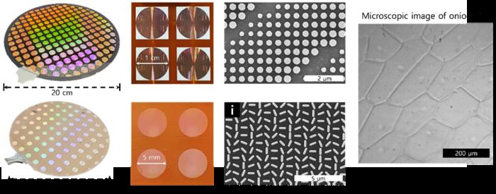
The research team recently achieved the mass production of metalenses for visible light region using deep ultraviolet photolithography, as published in the international journal Nature Materials. However, challenges emerged as the existing method demonstrated low efficiency in the infrared region. To address this limitation, the team developed a material with a high refractive index and low loss for the infrared region. This material was integrated into the established mass production process, resulting in the successful creation of a sizable infrared metalens with a 1cm diameter on an 8-inch wafer. Notably, the lens boasts a remarkable numerical aperture (NA) of 0.53, highlighting its exceptional light-collecting capability along with high resolution approaching the diffraction limit. The cylindrical structure further renders it polarization-independent, ensuring excellent performance regardless of the direction of light vibration.
In the second approach, the team employed nano imprinting, a process allowing for the printing of nanostructures using a mold. This process utilized the nanoimprint technique know-how, accumulated through collaborative research with RIST. This endeavor proved successful as the team managed to mass-produce a metalens with a 5-millimeter diameter, comprised of about a hundred million rectangular nanostructures on a 4-inch wafer. Notably, this metalens exhibited impressive performance, boasting an aperture of 0.53. Its rectangular structure showed polarization-dependent properties, effectively responding to the direction of light vibration.
Building upon this achievement, the team integrated a high-resolution imaging system to observe real samples such as onion epidermis, validating the possibility of commercializing metalenses. This research holds significance as it overcomes the limitations of the traditional one-by-one metalens production process. It not only facilitates the creation of optical devices with both polarization-dependent and -independent characteristics tailored to specific applications but also reduces the production cost of metalenses by up to 1,000 times.
Professor Junsuk Rho who led the research remarked, “We have achieved the precise and rapid production of high-performance metalenses on a wafer-scale, reaching centimeter dimensions.” He added, “Our aim is for this research to expedite the industrialization of metalenses, fostering the advancement of efficient optical devices and optical technologies.”
The research was conducted with support from a program of POSCO’s Industry-Academic Integrated Research Center and the STEAM Research Program, the RLRC Program, Nanomaterial Technology Development Program, and the Future Material Discovery Program of the Ministry of Science and ICT.
Journal
Laser & Photonics Review
DOI
10.1002/lpor.202300929
Article Title
Wafer-Scale Manufacturing of Near-Infrared Metalenses
Article Publication Date
10-Jan-2024


