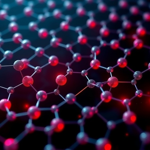
Graphene, a one-atom-thick sheet of carbon atoms arranged in a hexagonal lattice, has captivated scientists and engineers for over a decade due to its extraordinary physical properties. Renowned for its remarkable mechanical strength, flexibility, and phenomenal electrical conductivity, graphene has long been considered a material destined to revolutionize electronic devices. While graphene has already set records for electron mobility at room temperature, its performance under cryogenic conditions – that is, at extremely low temperatures – has until recently fallen short compared to the best semiconductor materials, particularly gallium arsenide (GaAs)-based systems. These systems have undergone decades of dedicated refinement, pushing them to the forefront of ultra-clean electronic behavior.
At the heart of this limitation lies a subtle but pervasive problem: electronic disorder caused by environmental imperfections. Graphene’s ultra-thin nature makes it highly vulnerable to minute fluctuations generated by charged impurities embedded in surrounding materials. These charged defects induce spatial variations in charge density, which manifest as so-called electron-hole puddles. Such inhomogeneities scatter electrons, hindering their ability to travel freely and drastically limiting mobility. This challenge has stood as a formidable barrier in harnessing graphene’s full potential for quantum and electronic applications that demand ultra-clean conductive platforms.
A recent breakthrough, however, has uncovered innovative strategies that surmount this historic obstacle, propelling graphene beyond the performance of state-of-the-art GaAs semiconductors even at cryogenic temperatures. Two parallel studies, spearheaded by teams at the National University of Singapore (NUS) and The University of Manchester, reveal complementary approaches to drastically reduce electronic disorder, thus unlocking record electron mobilities and enabling the observation of quantum phenomena under unprecedentedly mild conditions. These findings signal a paradigm shift in quantum materials research and the engineering of next-generation electronic devices.
Assistant Professor Alexey Berdyugin, a leading figure in the NUS Department of Materials Science and Engineering and co-corresponding author of both studies, explains that electron mobility quantifies how easily charge carriers navigate a material when subjected to an electric field. Higher mobility implies faster, less resistive electron flow which is essential for realizing ultra-fast, energy-efficient electronics. Specifically, materials exhibiting exceptionally high mobility are poised to transform advanced computing, sensing technologies, and emergent quantum platforms where coherent control of electrons is critical.
In the first pioneering study, researchers focused on inventing a method to protect graphene from the disruptive charge impurities prevalent in its environment by leveraging the concept of Coulomb screening. This involves strategically deploying additional graphene layers as ultra-thin electrostatic shields. By stacking two graphene sheets with a large twist angle relative to each other (between 10° and 30°), they ensured the layers remained electronically decoupled while still residing within a nanometer of each other. This unique geometric configuration allowed one graphene layer to be doped deliberately to behave like a metallic screen, effectively ironing out spatial charge fluctuations that scatter electrons in the primary graphene layer.
This twist-engineered Coulomb screening drastically reduced charge inhomogeneity to mere electrons per square micrometer, representing an order-of-magnitude improvement over previous designs. Such cleanliness enabled the direct observation of Landau quantization – a hallmark of quantum behavior in 2D electron systems – at magnetic field strengths as low as 5–6 milli-Tesla. By comparison, typical graphene devices require magnetic fields hundreds of times stronger to manifest similar quantum effects. The underlying physics stems from minimized scattering caused by long-range electric field fluctuations, pushing transport mobility values beyond 20 million cm²/Vs and surpassing the quantum mobility of the best GaAs electron gases.
The second study, conducted by Sir Andre Geim’s group at The University of Manchester with co-leadership by Dr. Daniil Domaretskiy, took an alternate yet equally transformative approach. Instead of an additional graphene layer, this team positioned graphene less than a nanometer away from a metallic graphite gate, separated by an ultrathin dielectric spacer comprising only three to four layers of hexagonal boron nitride. This proximity granted exceptionally strong Coulomb screening, sharply suppressing charge disorder and bringing the electron-hole puddle density down to around 3×10⁷ cm⁻² — the equivalent of one extraneous charge per 100 million carbon atoms near charge neutrality.
The devices fabricated using this proximity screening technique demonstrated Hall mobilities surpassing 60 million cm²/Vs, eclipsing even the most sophisticated GaAs systems. Moreover, the quantum Hall effect, ordinarily observed at magnetic fields of several Tesla, was clearly visible at fields below 5 milli-Tesla. Equally striking were Shubnikov–de Haas oscillations—another quantum signature—which appeared at an astonishingly low field of just 1 milli-Tesla, a value comparable to Earth’s intrinsic magnetic field strength.
Together, these two complementary methodologies tackle the inherent problem of charged defect-induced disorder from different angles. The twist-angle graphene stacking design offers an elegant and highly tunable means of screening, allowing researchers to explore a broad parameter space in terms of electronic interaction and coupling. On the flip side, the proximity metallic screening method presents a clean, direct probe of intrinsic graphene properties without additional parasitic signals from the screening layer. This latter approach enables pristine observation of quantum phenomena like clean Quantum Hall plateaus at remarkably low magnetic fields.
Assistant Professor Berdyugin underscores the significance of these achievements, emphasizing how this expanded experimental toolkit opens new avenues for fundamental inquiry and technological innovation. The unparalleled purity achieved in these graphene devices is poised to accelerate progress in quantum metrology, where precision measurements rely on stable quantum Hall effects, as well as in ultra-sensitive electronic sensors that base their functionality on faultless charge transport. Furthermore, the record mobilities enabled here are vital for advancing next-generation electronics optimized for speed and energy conservation.
Looking toward the future, the research teams plan to extend these methods to more intricate graphene-based heterostructures, especially those hosting moiré quantum materials. These complex structures exhibit a plethora of correlated electron phenomena, including unconventional superconductivity and exotic many-body states, which have captivated condensed matter physicists worldwide. The breakthroughs in controlling disorder and enhancing mobility promise to provide cleaner platforms for probing these enigmatic quantum phases.
In reflection, this watershed moment in graphene research dramatically alters the boundaries of what was thought possible. The immense reduction in electronic disorder achieved by these novel screening techniques not only sets new world records but also fundamentally changes the landscape of 2D material physics. As Mr. Ian Babich, a doctoral researcher involved in the work, remarks, “The performance ceiling we now break opens up an entire new physics landscape, inspiring further exploration and technological breakthroughs.”
These findings exemplify how a meticulous combination of material engineering, precise nanofabrication, and fundamental physics theory can culminate in unprecedented scientific and technological milestones. With the promise of ultra-clean, ultra-fast graphene electronics and scalable quantum devices on the horizon, the age of graphene as a field-defining two-dimensional material is truly entering a new era of discovery and application.
Subject of Research: Not applicable
Article Title: Milli-Tesla quantization enabled by tuneable Coulomb screening in large-angle twisted graphene
News Publication Date: 11-Aug-2025
Web References:
https://www.nature.com/articles/s41467-025-62492-5
https://www.nature.com/articles/s41586-025-09386-0
Image Credits: College of Design and Engineering at NUS
Keywords
Two dimensional materials, Physics, Solid state physics, Transport phenomena, Quantum matter
Tags: cryogenic performance of grapheneelectron mobility in grapheneelectron-hole puddles in materialselectronic disorder in materialsenhancing graphene conductivityenvironmental imperfections in graphenegallium arsenide semiconductor comparisongraphene electronic propertiesgraphene revolution in electronicsquantum applications of graphenesemiconductor technology advancementsultra-clean electronic systems


