
Researchers at Nokia Bell Labs have unveiled an innovative optical memory technology, known as the programmable photonic latch, which promises to revolutionize data storage in optical processing systems. This groundbreaking unit is both fast and scalable, offering a solution that could significantly enhance the efficiency of volatile memory applications utilizing silicon photonics. The implications of this achievement could reshape the landscape of data storage and processing, further bridging the gap between optical communication and digital storage.
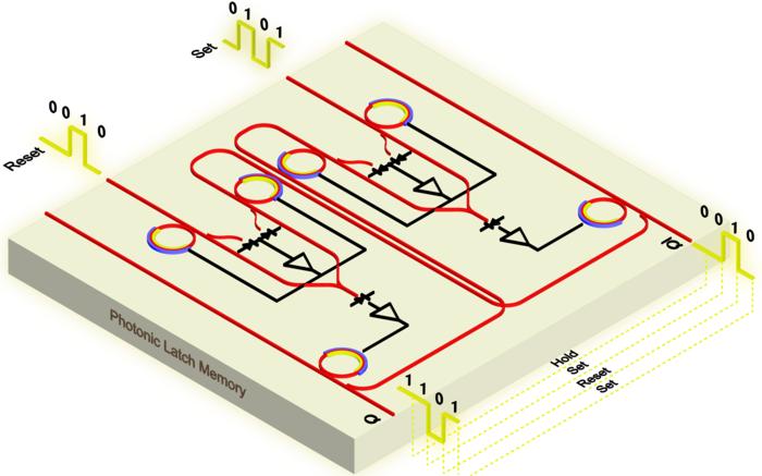
One of the most intriguing aspects of the programmable photonic latch is its ability to temporarily hold data in optical systems. This memory unit is built around the concept of a set-reset latch, a simple memory element that can toggle between two states, representing binary data. This is critical in optical computing applications where speed and energy efficiency are paramount, making the programmable latch a potential game-changer in the field of memory technology.
Farshid Ashtiani, a lead researcher in the study, emphasizes the significance of this new technology in the context of existing optical communication and computing systems. Historically, data storage has leaned heavily on electronic solutions, which, while effective, often lag behind in speed and efficiency when compared to optical counterparts. Ashtiani notes that integrating a fast optical memory solution like the programmable photonic latch will not only streamline operations but also reduce energy consumption, creating a more sustainable framework for future optical processing systems.
The researchers detailed their findings in a recent publication in the journal Optics Express, outlining a proof-of-concept experiment that showcases the capabilities of the programmable photonic latch. This experiment leveraged a silicon photonic platform to demonstrate the latch’s optical set and reset features, providing complementary outputs while maintaining scalability and wavelength division multiplexing (WDM) compatibility. Such characteristics bode well for the advanced optical processing systems of tomorrow, as they promise increased speed and efficiency.
The utilization of silicon photonics distinguishes the programmable latch from previous optical memory technologies. Traditionally, many optical memory systems required cumbersome and costly setups, often incorporating specialized materials that are not widely accessible in the commercial domain. By employing silicon photonic micro-ring modulators, the researchers have constructed a more efficient and economically feasible memory solution. This allows for greater scalability, ultimately enabling a wider adoption of optical memory technologies in everyday applications.
One of the standout features of the programmable photonic latch is its scalability. Each memory unit operates with its own input light source, allowing multiple units to function simultaneously without interference. This independent operation mitigates concerns about signal degradation that can arise when multiple memory units are interconnected. As a result, the scalability offered by this new technology could pave the way for the creation of larger and more sophisticated memory systems.
In addition to scalability, the photonic memory unit displays impressive wavelength selectivity. This attribute not only enhances the memory unit’s compatibility with WDM systems, but also facilitates multi-bit data storage within a single unit. Moreover, the memory’s response time is remarkably fast, clocked at mere tens of picoseconds—outmatching current advanced digital systems and emphasizing the potential for high-speed optical data storage.
The experimental design of the study involved the implementation of universal logic gates to establish the functionality of the optical latch. Researchers conducted comprehensive tests under varying input conditions to ensure reliability. The results were promising, with the gates and latches performing their respective operations—set, reset, and hold—accurately, even amidst fluctuations in input power. This robustness underlines the practical application potential of the programmable photonic latch.
Looking toward the future, the team at Nokia Bell Labs is dedicated to advancing this photonic memory technology. Plans are in place to scale up the current setup to accommodate a greater number of memory units. They aim to fabricate dedicated photonic memory chips that can seamlessly integrate into existing systems. Furthermore, integrating electronic controls within a single manufacturing process is a critical goal, as it would enhance the overall functionality and appeal of the photonic memory unit in commercial applications.
Through continued research and development, the programmable photonic latch could address several long-standing challenges in the realm of optical processing. The researchers are committed to making this technology practical and accessible, and their vision includes creating higher on-chip memory density using WDM compatibility. This could transform not only how data is processed but also how it is stored on a fundamental level.
Ashtiani and his team envision a future where optical memory is no longer an afterthought but an integral component of computing systems. They note that large language models, like ChatGPT, depend on rapid calculations involving vast amounts of data—specifically, operations like addition and multiplication performed iteratively. Incorporating high-speed optical memory could significantly accelerate these processes, pushing the boundaries of what is currently achievable in machine learning and artificial intelligence applications.
While the prospect of commercial optical computers remains a distant ambition, the development of technologies like the programmable photonic latch represents a vital stepping stone in that journey. With this innovative memory technology, researchers at Nokia Bell Labs are poised to contribute to a new era of computational efficiency, scalability, and speed that is entirely consonant with the demands of a data-intensive world.
In conclusion, the programmable photonic latch signifies a pivotal development in optical memory technology. With its fast response times, scalable architecture, and compatibility with existing optical systems, it holds the promise of transforming how data is stored and processed in the future.
Subject of Research: Programmable photonic latch memory technology
Article Title: Programmable photonic latch memory
News Publication Date: 23-Jan-2025
Web References: https://opg.optica.org/oe/home.cfm
References: F. Ashtiani, “Programmable photonic latch memory,” Opt. Express, 33, XXXX (2024). DOI: 10.1364/OE.536535
Image Credits: Credit: Farshid Ashtiani, Nokia Bell Labs
Keywords
1. Photonic memory
2. Data storage
3. Silicon photonics
4. Optical processing
5. High-speed computing
6. Volatile memory
7. Wavelength division multiplexing
8. Scalable memory systems
9. Optical interconnects
10. Machine learning
11. Artificial intelligence
12. Memory technology
Tags: Okay


