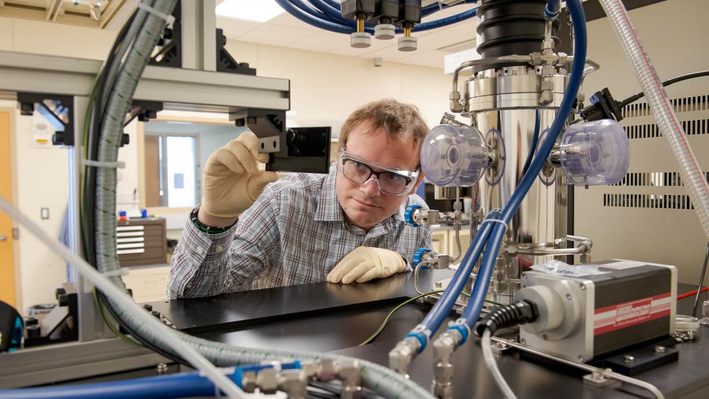
Credit: (Image by Argonne National Laboratory.)
Claiming that something has a defect normally suggests an undesirable feature. That’s not the case in solid-state systems, such as the semiconductors at the heart of modern classical electronic devices. They work because of defects introduced into the rigidly ordered arrangement of atoms in crystalline materials like silicon. Surprisingly, in the quantum world, defects also play an important role.
Researchers at the U.S. Department of Energy’s (DOE) Argonne National Laboratory, the University of Chicago and scientific institutes and universities in Japan, Korea and Hungary have established guidelines that will be an invaluable resource for the discovery of new defect-based quantum systems. The international team published these guidelines in Nature Reviews Materials.
“We are especially proud of our guidelines because intended users extend from veteran quantum scientists to researchers in other fields and graduate students hoping to join the quantum workforce.” — Gary Wolfowicz, assistant scientist in Argonne’s Center for Molecular Engineering and Materials Science division, along with the University of Chicago Pritzker School of Molecular Engineering
Such systems have possible applications in quantum communications, sensing and computing and thereby could have a transformative effect on society. Quantum communications could distribute quantum information robustly and securely over long distances, making a quantum internet possible. Quantum sensing could achieve unprecedented sensitivities for measurements with biological, astronomical, technological and military interest. Quantum computing could reliably simulate the behavior of matter down to the atomic level and possibly simulate and discover new drugs.
The team derived their design guidelines based on an extensive review of the vast body of knowledge acquired over the last several decades on spin defects in solid-state materials.
“The defects that interest us here are isolated distortions in the orderly arrangement of atoms in a crystal,” explained Joseph Heremans, a scientist in Argonne’s Center for Molecular Engineering and Materials Science division, as well as the University of Chicago Pritzker School of Molecular Engineering.
Such distortions might include holes or vacancies created by the removal of atoms or impurities added as dopants. These distortions, in turn, can trap electrons within the crystal. These electrons have a property called spin, which acts as an isolated quantum system.
“Spin being a key quantum property, spin defects can hold quantum information in a form that physicists call quantum bits, or qubits, in analogy with the bit of information in classical computing,” added Gary Wolfowicz, assistant scientist in Argonne’s Center for Molecular Engineering and Materials Science division, along with the University of Chicago Pritzker School of Molecular Engineering.
For several decades, scientists have been studying these spin defects to create a broad array of proof-of-concept devices. However, previous research has only focused on one or two leading candidate qubits.
“Our field has had a somewhat narrow focus for many years,” said Christopher Anderson, a postdoctoral scholar in the University of Chicago Pritzker School of Molecular Engineering. “It was like we only had a few horses in the quantum race. But now we understand that there are many other quantum horses to back, and exactly what to look for in those horses.”
The team’s guidelines encompass the properties of both the defects and the material selected to host them. The key defect properties are spin, optical (for example, how light interacts with the spin of the trapped electrons), and charge state of the defect.
Possible solid-state materials include not only the already well-studied few like silicon, diamond and silicon carbide but other more recent entries like various oxides. All these materials have different advantages and disadvantages laid out in the guidelines. For example, diamond is clear and hard, but expensive. On the other hand, silicon is easy to make devices with at low cost, but is more affected by free charges and temperature.
“Our guidelines are there for quantum scientists and engineers to assess the interplay between the defect properties and the selected host material in designing new qubits tailored to some specific application,” Heremans noted.
“Spin defects have a central role to play in creating new quantum devices, whether they be small quantum computers, the quantum internet, or nanoscale quantum sensors,” continued Anderson. “By drawing upon the extensive knowledge on spin defects to derive these guidelines, we have laid the groundwork so that the quantum workforce — now and in the future — can design from the ground up the perfect qubit for a specific use.”
“We are especially proud of our guidelines because intended users extend from veteran quantum scientists to researchers in other fields and graduate students hoping to join the quantum workforce,” said Wolfowicz.
The work also establishes the groundwork for designing scalable semiconductor quantum devices and dovetails well with Q-NEXT, a DOE-funded quantum information science research center led by Argonne. Q-NEXT’s goal includes establishing a semiconductor quantum “foundry” for developing quantum interconnects and sensors.
“Our team’s guidelines will act as a blueprint to help direct the Q-NEXT mission in designing the next generation of quantum materials and devices,” said David Awschalom, senior scientist in Argonne’s Materials Science division, Liew Family Professor of Molecular Engineering at the University of Chicago Pritzker School of Molecular Engineering, and director of both the Chicago Quantum Exchange and Q-NEXT. “When it comes to quantum technologies with spins, this work sets the stage and informs the field how to move forward.”
The team’s guidelines appear in a paper entitled “Qubit guidelines for solid-state spin defects” and published in Nature Reviews Materials. In addition to Heremans, Wolfowicz, Anderson and Awschalom, authors include Shun Kanai (Tohoku University, Japan), Hosung Seo (Ajou University, Korea), Adam Gali (Budapest University of Technology and Economics, Hungary) and Giulia Galli (Argonne and University of Chicago).
This research was primarily supported by the DOE Office of Science.
Argonne National Laboratory seeks solutions to pressing national problems in science and technology. The nation’s first national laboratory, Argonne conducts leading-edge basic and applied scientific research in virtually every scientific discipline. Argonne researchers work closely with researchers from hundreds of companies, universities, and federal, state and municipal agencies to help them solve their specific problems, advance America’s scientific leadership and prepare the nation for a better future. With employees from more than 60 nations, Argonne is managed by UChicago Argonne, LLC for the U.S. Department of Energy’s Office of Science.
The U.S. Department of Energy’s Office of Science is the single largest supporter of basic research in the physical sciences in the United States and is working to address some of the most pressing challenges of our time. For more information, visit https:/
###
Media Contact
Diana Anderson
[email protected]
Original Source
https:/
Related Journal Article
http://dx.


