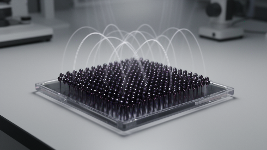
A tiny chip no bigger than a fingernail can now warn of dangerous high-frequency electromagnetic fields without a battery, a wire, or a single electronic component. Researchers at KIST Europe in Saarbrücken, Delft University of Technology, and the University of Science and Technology in Daejeon have built a passive sensor that converts incoming radio-frequency energy directly into a visible optical signal, drawing all of its power from the very radiation it detects. The device, described in Communications Engineering, relies on nothing more exotic than a common liquid crystal, a fine mesh of nickel wires, and two sheets of polarizing film, yet it changes color from bright to dark in the presence of an alternating magnetic field, a change visible to the naked eye under ordinary ambient light.
The motivation behind the work is rooted in a growing tension of modern life. High-frequency electromagnetic fields are everywhere, emitted by power lines, communication systems, imaging technologies, and the dense infrastructure of 5G and 6G wireless networks and satellite communications. While short-term exposure within prescribed safety limits is generally considered minimal risk, long-term exposure to high-frequency radiation has been associated with detrimental effects on human health and ecosystems. In industrial settings, local field intensities can spike unexpectedly when multiple sources overlap or when equipment malfunctions, yet most monitoring today relies on bulky, powered instruments that cannot be worn or embedded cheaply in every device that might pose a hazard.
There is also a security dimension. High-frequency fields are the physical medium of electromagnetic pulse weapons, which can be used defensively but also maliciously in cyberterrorism. Real-time, in-situ detection of destructive electromagnetic fields would significantly enhance risk management for command-and-control systems and battlefield operations. Drone warfare, in particular, demands simple onboard microsensors capable of detecting and alarming potential electromagnetic attacks. Existing sensor technologies, from Hall effect devices and anisotropic magnetoresistance elements to giant magnetoresistance and spin-dependent tunneling sensors, offer compact designs with medium-to-high accuracy, but they all require detection electronics powered by external energy supplies, limiting their mobility and their usefulness in passive, wearable formats.
The new chip takes a radically different approach by exploiting a magnetothermal mechanism. At its heart is a thin, flat cell filled with the thermotropic liquid crystal 4-cyano-4′-pentylbiphenyl, better known as 5CB, a rod-like nematic compound that has served as a model material since its first synthesis in 1973. Embedded within the liquid crystal matrix is a network of thin ferromagnetic wires, a 50-mesh nickel gauze with wires roughly 50 micrometers in diameter. Both sides of the chip are laminated with polymer-based polarizer films aligned at 90 degrees to each other, forming crossed polarizers in direct contact with the liquid crystal. The assembled device measures about one centimeter square, weighs less than 0.3 grams, and has a Young’s modulus on the order of tens of kilopascals, making it flexible and light enough for integration into smart glasses or miniature unmanned aerial vehicles.
The physics of the sensing process unfolds in two coupled steps. First, when an external alternating magnetic field exceeds roughly 6 millitesla at the tested frequency of 125 kilohertz, the time-varying field induces eddy currents in the conductive nickel mesh, generating Joule heating. Because nickel has a high relative permeability, it concentrates the magnetic field, increasing the induced currents and heating efficiency compared with a non-magnetic mesh. A second mechanism, magnetic hysteresis loss, contributes additional heat that occurs only in ferromagnetic materials and is proportional to the area under the magnetization loop. The heating power scales with the square of the product of field strength and frequency, which means even modest increases in either parameter dramatically accelerate the response.
Second, the heat generated in the mesh diffuses into the surrounding liquid crystal. Once the local temperature surpasses the clearing point of 5CB at about 35 degrees Celsius, the material undergoes a reversible phase transition from the nematic phase, in which the rod-like molecules are quasi-one-dimensionally ordered, to the isotropic phase, in which they are globally disordered. This transition changes the optical properties of the film dramatically. In the nematic, field-off state, the unaligned liquid crystal exhibits strong birefringence between the crossed polarizers, so the chip transmits ambient light and appears bright. In the isotropic, field-on state, birefringence vanishes and transmittance drops to near zero, so the chip turns dark. No separate transducer is needed to convert temperature into an optical signal; the phase transition itself is the readout.
In experiments, the researchers placed the chip at the center of a Helmholtz coil driven by an induction heater power supply and filmed its response with a digital camera positioned about 1.5 meters away to shield the camera electronics from interference. When a field of 125 kilohertz and up to 30 millitesla was applied, optically dark domains appeared near the chip center, grew into a ring-like pattern, and rapidly spread to cover most of the display. When the field was switched off, the dark domain gradually shrank and disappeared as heat dissipated by natural convection, completing a full on-off cycle in roughly ten seconds at room temperature. The response time upon induction heating was as fast as 30 milliseconds, while recovery took tens of seconds. The chip showed remarkably high stability and repeatability over more than ten consecutive field pulses.
To understand and predict this behavior, the team built a finite element model in COMSOL Multiphysics that coupled electromagnetic induction with heat transfer and the latent-heat-mediated phase transition. The simulations closely matched the experimental data, predicting the characteristic transition times and optical switching behavior across a wide range of field strengths, generally falling within the standard deviation of the measurements. The model revealed that the onset of the nematic-to-isotropic transition follows a line of constant field-frequency product, suggesting the system operates in the low-frequency regime where heating power scales as the square of that product. The researchers also found that sensitivity increases with the volume fraction of the nickel mesh: a denser mesh generates heat faster and shortens response times, though it also stores more thermal energy and lengthens recovery. Skin-depth effects, estimated at about 30 micrometers at 125 kilohertz, comparable to the wire diameter, add a further frequency-dependent wrinkle to the design space.
The material choices are deliberately pragmatic. 5CB is cheap, easy to handle, and stable at room temperature thanks to long-term supercooling of its nematic melt, and its low viscosity, volatility, and toxicity make it practical for real devices. Its clearing temperature of 35 degrees Celsius suits temperate climates, but the authors note that alternative or blended liquid crystals with higher transition temperatures, such as MBBA at 47 degrees Celsius, could extend operation to warmer subtropical environments, while lower-transition materials could serve aerospace applications. Tuning the mesh geometry, wire diameter, or liquid crystal composition offers further control over sensitivity and response time, and coating the wires with anchoring agents could better align the liquid crystal molecules for improved performance.
The combination of extreme simplicity, millimeter-scale dimensions, lightweightness, passive operation, and a robust visual readout positions this chip as a promising candidate for ultra-low-power wearable technologies, mobile platforms, and electronic warfare systems. Because the sensor is fundamentally independent of electronics, it is also inherently resistant to external field-induced signal noise that plagues conventional detectors. The researchers caution that the thermally driven mechanism is slower than the millisecond intrinsic reorientation of the liquid crystal itself, spanning from several milliseconds at high fields to tens of seconds near the detection limit, and that future work will explore faster liquid crystal formulations inspired by electro-optical sensing modes. Even so, the demonstration that electromagnetic radiation can be caught, converted, and displayed by a chip with no power source of its own marks a striking step toward a world where hazard warnings are woven invisibly into the fabric of everyday objects.
Subject of Research: Passive liquid crystal sensor chip for detecting high-frequency electromagnetic fields
Article Title: Electronics-free, ultra-low-power, wearable sensor chip for high-frequency electromagnetic field detection
Article References: Mohizin, A., Abelmann, L., & Sung, B. (2026). Electronics-free, ultra-low-power, wearable sensor chip for high-frequency electromagnetic field detection. Communications Engineering, 5(1), Article 170. https://doi.org/10.1038/s44172-026-00800-7
Image Credits: AI Generated
DOI: 10.1038/s44172-026-00800-7
Keywords: liquid crystals, electromagnetic field sensor, wearable technology, magnetothermal effect, nickel mesh, 5CB, passive sensing, radio-frequency detection, phase transition, electronics-free, electromagnetic pulse, birefringence
News Source: Faith Mcneil. (October 9, 2026). Battery-free liquid crystal chip glows dark when dangerous electromagnetic fields strike. Scienmag.