Credit: by Wei Jiang, Tan Zheng, Binmin Wu, Hanxue Jiao, Xudong Wang, Yan Chen, Xiaoyu Zhang, Meng Peng, Hailu Wang, Tie Lin, Hong Shen, Jun Ge, Weida Hu, Xiaofeng Xu, Xiangjian…
Photodetectors have always paly the important role in the national economy and national defense field. The advanced photodetectors demand for the higher performance in response rate, broad spectrum, detectivity and other special functions like polarization detection and two-color detection. However, the limited exploitation of traditional materials or single detection mechanism faces the challenge of losing competitiveness. Inducing novel materials and integrating multiple detection mechanisms may create a detector with excellent comprehensive performance, and take the dominant in the next generation photodetector.
In a new paper published in Light Science & Application, a team of scientists, led by Professor Jianlu Wang from State Key Laboratory of Infrared Physics, Shanghai Institute of Technical Physics, Chinese Academy of Sciences, China, and co-workers have developed a versatile photodetector integrating photovoltaic and bolometric effects. It is a heterostructure composed of molybdenum telluride (MoTe2) and vanadium dioxide (VO2), in which MoTe2 acts as transferable semiconductor and VO2 acts as bolometric materials.
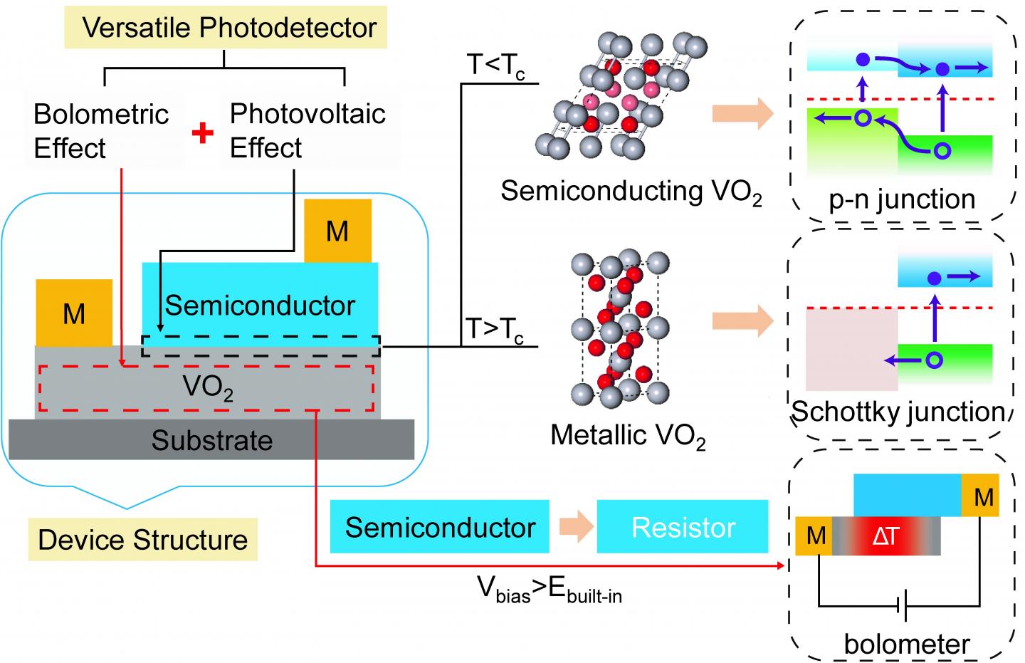
Based on this structure, the device achieves three different functional modes including i) p-n junction, exhibits ultrasensitive detection (450 nm – 2 μm) with the dark current down to 0.2 pA and response time of 17 μs, ii) Schottky junction, work stable under extreme condition as high temperature of 400 K, iii) bolometer, shows ultrabroad spectrum detection exceeding to 10 μm. The flexible switch between three modes make it a potential candidate for next-generation photodetectors from visible to long-wave infrared radiation (LWIR). This dual-mechanism integration strategy opens up a novel development path to advanced optoelectronic devices. These scientists summarize the operation principles of their versatile photodetector:
p-n junction mode:
When the MoTe2 is transferred to the top of VO2 at room temperature, a space charge region (SCR) appears at the interface of VO2 and MoTe2 as the carriers swept out by the built-in electric field. Electron-hole pairs are generated in the SCR by electron transition under light illumination. Because of the photovoltaic effect, the electrons and holes are separated and collected by electrodes, which accounts for the source of photocurrent. To minimize the dark current, this mode are works at zero bias. The separation process is driven by built-in field, the response rare is rather fast than other detection mechanism. Additionally, VO2 is a narrow bandgap semiconductor, the p-n junction mode can response to light radiation of 2 μm.
Schottky junction mode:
VO2 is a typical phase transition material with metal-insulator-transition (MIT) near room temperature (340K). The device transforms to Schottky junction when VO2 become metallic at the temperature exceeding MIT temperature. Although the dark current is increased compared to room temperature, the device is still capable of photodetection from visible to near infrared radiation. This mode can be used industrial inspection as high as 400 K, is an extension of the traditional detector.
Bolometer mode:
VO2 is classical materials in bolometer industry because of its large temperature coefficient of resistance (TCR). As we know, when the forward bias is larger than built-in electric field, p-n junction can be considered as a resistor. Therefore, the device transforms into a bolometer. The bolometer absorbs the heat energy and is not selective to the wavelength of radiation, therefore, the device can be used to detect mid-wave infrared radiation (MWIR) and LWIR.
###
Media Contact
Jianlu Wang
[email protected]
Related Journal Article
http://dx.


