Credit: ©Science China Press
If a semiconductor crystal is doped with n-type dopants in one region and with p-type dopants in another region, a p-n junction configuration is formed. p-n junctions are fundamental building units of light emitting diodes, solar cells and other semiconductor transistors. p-n junctions in nano-structures are also expected to be the fundamental units of next generation nano-devices. However, due to the strong attraction between them, n-type dopants and p-type dopants tend to form neutral pairs. As a result, the p-n junction fails. To prevent such attraction between n-type dopants and p-type dopants, heterostructures are introduced, where one semiconductor material is doped with n-type dopants while the other is doped with p-type dopants, and the interface between two different semiconductor materials acts as an energy barrier between n-type dopants and p-type dopants. Indeed, the usage of heterostructures stands for a paradigm for the material design of p-n junction. Recently, similar p-n junction configurations are also possible for nanowire heterostructures such as co-axial core-shell nanowires. However, there are several limitations in nanowire heterostructures. For example, the synthesis of core-shell nanowires usually involves a two-step process, which costs extra expense. Often the shell of the obtained nanowire heterostructure is polycrystalline. Such imperfection goes ill with the transports of carriers. Furthermore, the interface between the core and shell also introduces detrimental deep centers that largely hinder the device efficiency.
Can we make p-n junctions with single crystalline nanowires? Frankly, the answer will be “No” if one thinks the problem intuitively. Indeed, similar to the bulk, p-type dopants and n-type dopants in a codoped single crystalline nanowire also feel strong Coulomb attraction. Without an interface, how can we overcome such attraction? It requires an effective modulation/control of the spatial occupation sites, i.e., spatial distribution, of dopants. In fact, this is one of the long-standing and fundamental issues regarding doping in semiconductor. From the point of view of materials engineering, this can be attributed to the failure of conventional approaches such as hydrostatic, biaxial and uniaxial stresses on the modulation of the spatial distribution of dopants. However, since all these mentioned distortions are uniform, can we employ some inhomogeneous ones, such as twisting? In fact, twisting of structures represents a focus of recent condensed matter physics research in low dimensions.
In a new paper published in National Science Review, a team of scientists from Beijing Normal University, the Chinse University of Hong Kong, and Beijing Computational Science Research Center present their theoretical advances of codoped Si nanowire under twisting. They employ both microscopic simulations based on the generalized Bloch theorem and analytical modeling based on the bond orbital theory to conduct the study and deliver the physics behind.
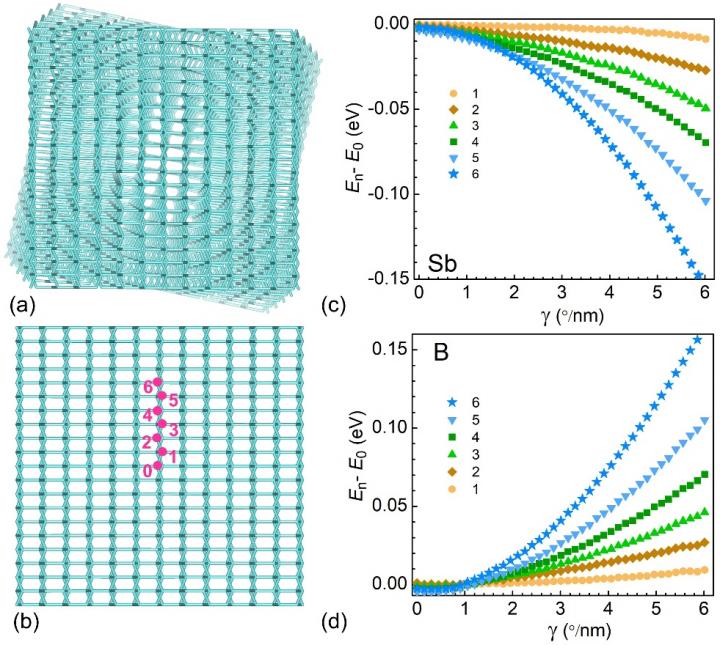
Interestingly, twisting has substantial impact on distribution of dopants in nanowires. From the displayed figure, in a twisted Si nanowire, a dopant of larger atomic size (Such as Sb) has a lower formation energy if it occupies an atomic site closer to nanowire surface; On the opposite, a dopant of smaller atomic size (Such as B) has a lower formation energy if it occupies an atomicsites around the nanowire core. According to their calculations, it is possible to separate n-type and p-type dopants in the codoped nanowire with proper choices of codoping pairs, e.g., B and Sb. A bond orbital analysis reveals that it is the twist-induced inhomogeneous shear strain along nanowire radial dimension that drives the effective modulation. These findings are fully supported by density-functional tight-binding based generalized Bloch theorem simulations.
This new strategy largely simplifies the manufactory process and lowers the manufactory costs. If the twisting is applied when the device is in working mode, the recombination of different types of dopants is largely suppressed. Even if the twisting is removed when the device is in working mode, due to the limited diffusion, the recombination is still difficult.
###
This research received funding from National Natural Science Foundation of China, Beijing Normal University, HKRGC funding, and the Chinese University of Hong Kong.
See the article:
Dong-Bo Zhang Xing-Ju Zhao, Gotthard Seifert, Kinfai Tse, and Junyi Zhu,
Twist-Driven Separation of p-type and n-type Dopants in Single Crystalline Nanowires Natl Sci Rev 2019; 10.1093/nsr/nwz014
https:/
The National Science Review is the first comprehensive scholarly journal released in English in China that is aimed at linking the country’s rapidly advancing community of scientists with the global frontiers of science and technology. The journal also aims to shine a worldwide spotlight on scientific research advances across China.
Media Contact
Bei Yan
[email protected]
Related Journal Article
http://dx.


