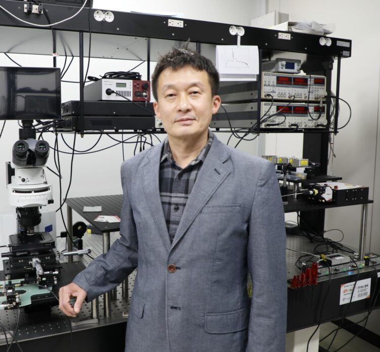
Scientists devise a 2D-material-based stacked structure with applications in reducing computing power consumption

Credit: DGIST
2D materials have been popular among materials scientists owing to their lucrative electronic properties, allowing their applications in photovoltaics, semiconductors, and water purification. In particular, the relative physical and chemical stability of 2D materials allow them to be “stacked” and “integrated” with each other. In theory, this stability of 2D materials enables the fabrication of 2D material-based structures like coupled “quantum wells” (CQWs), a system of interacting potential “wells,” or regions holding very little energy, which allow only specific energies for the particles trapped within them. CQWs can be used to design resonant tunneling diodes, electronic devices that exhibit a negative rate of change of voltage with current and are crucial components of integrated circuits. Such chips and circuits are integral in technologies that emulate neurons and synapses responsible for memory storage in the biological brain.
Proving that 2D materials can indeed be used to create CQWs, a research team led by Myoung-Jae Lee Ph.D. of Daegu Gyeongbuk Institute of Science and Technology (DGIST) designed a CQW system that stacks one tungsten disulfide (WS2) layer between two hexagonal boron nitride (hBN) layers. “hBN is a nearly ideal 2D insulator with high chemical stability. This makes it a perfect choice for integration with WS2, which is known to be a semiconductor in 2D form”, explains Prof. Lee. Their findings are in published in ACS Nano.
The team measured the energy of excitons–bound systems comprising an electron and an electron hole (absence of electron)–and trions (electron-bound exciton) for the CQW and compared them to that for bilayer WS2 structures to identify the effect of WS2-WS2 interaction. They also measured the current-voltage characteristics of a single CQW to characterize its behavior.
They observed a gradual decrease in both the exciton and trion energy with an increase in the number of stakes, and an abrupt decrease in the bilayer WS2. They attributed these observations to a long-range inter-well interaction and strong WS2-WS2 interactions in absence of hBN, respectively. The current-voltage characteristics confirmed that it behaves like a resonant tunneling diode.
So, what implications do these results have for the future of electronics? Prof. Lee summarizes, “We can use resonant tunneling diodes for making multivalued logic devices that will reduce circuit complexity and computing power consumptions considerably. This, in turn, can lead to the development of low-power electronics.”
These findings are sure to revolutionize the electronics industry with extreme low power semiconductor chips and circuits, but what is more exciting is where these chips can take us, as they can be employed in applications that mimic neurons and synapses, which play a role in memory storage in the biological brain. This “2D perspective” may thus be the next big thing in artificial intelligence!
###
Reference
Authors: Myoung-Jae Lee1, David H. Seo2, Sung Min Kwon3, Dohun Kim1,Youngwook Kim1,Won Seok Yun1,Jung-Hwa Cha1,Hyeon-Kyo Song4,Shinbuhm Lee1,MinKyung Jung1,Hyeon-Jun Lee1,June-Seo Kim1,Jae-Sang Heo5,Sunae Seo4 and Sung Kyu Park3
Title of original paper: Measurement of Exciton and Trion Energies in Multistacked hBN/WS2 Coupled Quantum Wells for Resonant Tunneling Diodes
Journal: ACS Nano
DOI: 10.1021/acsnano.0c08133
Affiliations:
- Daegu Gyeongbuk Institute of Science and Technology (DGIST)
- PSK Inc.
- Chung-Ang University
- Sejong University
- University of Connecticut School of Medicine
*Corresponding author’s email:
[email protected] ,
[email protected]
About Daegu Gyeongbuk Institute of Science and Technology (DGIST)
Daegu Gyeongbuk Institute of Science and Technology (DGIST) is a well-known and respected research institute located in Daegu, Republic of Korea. Established in 2004 by the Korean Government, the main aim of DGIST is to promote national science and technology, as well as to boost the local economy.
With a vision of “Changing the world through convergence”, DGIST has undertaken a wide range of research in various fields of science and technology. DGIST has embraced a multidisciplinary approach to research and undertaken intensive studies in some of today’s most vital fields. DGIST also has state-of-the-art-infrastructure to enable cutting-edge research in materials science, robotics, cognitive sciences, and communication engineering.
Website: https:/
About the author
Myoung-Jae Lee received his B.S., M.S., and Ph.D. degrees in electronic engineering from Kyung Hee University, Korea, in 1995, 1998, and 2003, respectively. In 1999, he joined Hynix, Korea, where he researched the development of DRAM. In 2003, he was hired at Samsung Electronics, Yongin, Korea, where he researched resistance change memory for the next-generation nonvolatile memory. Since 2015, he has been with DGIST, Daegu, Korea, where he is currently leading research on the emerging memory devices for neuromorphic computing. His research interests include multi-valued logic and artificial synaptic devices for ultra-low-power artificial intelligence semiconductors.
Media Contact
Kwanghoon Choi
[email protected]
Original Source
https:/
Related Journal Article
http://dx.


