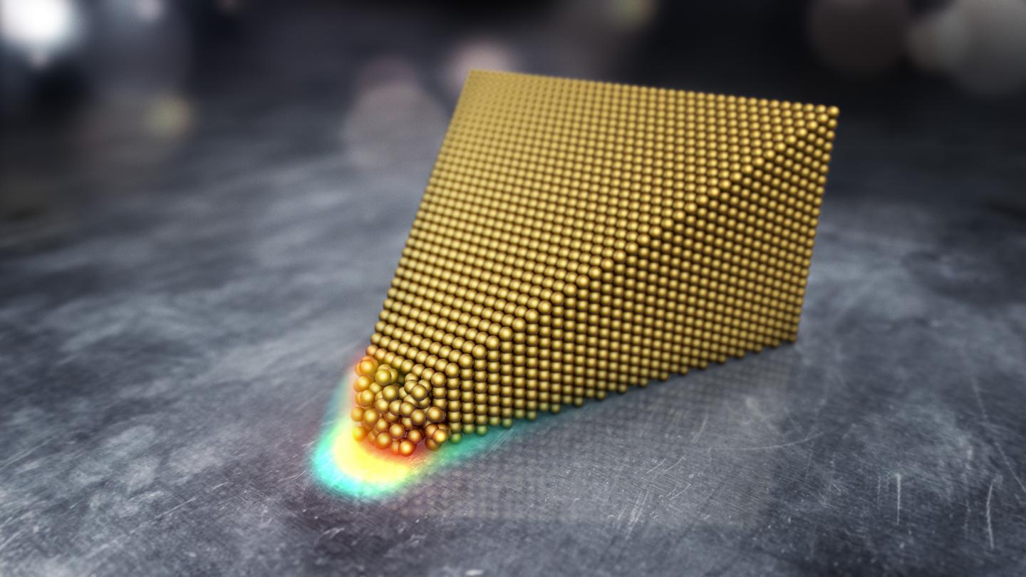
Credit: Alexander Ericson
When the tension rises, unexpected things can happen – not least when it comes to gold atoms. Researchers from, among others, Chalmers University of Technology, Sweden, have now managed, for the first time, to make the surface of a gold object melt at room temperature.
Ludvig de Knoop, from Chalmers' Department of Physics, placed a small piece of gold in an electron microscope. Observing it at the highest level of magnification and increasing the electric field step-by-step to extremely high levels, he was interested to see how it influenced the gold atoms.
It was when he studied the atoms in the recordings from the microscope, that he saw something exciting. The surface layers of gold had actually melted – at room temperature.
"I was really stunned by the discovery. This is an extraordinary phenomenon, and it gives us new, foundational knowledge of gold," says Ludvig de Knoop.
What happened was that the gold atoms became excited. Under the influence of the electric field, they suddenly lost their ordered structure and released almost all their connections to each other. Upon further experimentation, the researchers discovered that it was also possible to switch between a solid and a molten structure.
The discovery of how gold atoms can lose their structure in this way is not just spectacular, but also groundbreaking scientifically. Together with the theoretician Mikael Juhani Kuisma, from the University of Jyväskylä in Finland, Ludvig de Knoop and colleagues have opened up new avenues in materials science. The results are now published in the journal Physical Review Materials.
Thanks to theoretical calculations, the researchers are able to suggest why gold can melt at room temperature. Possibly, the surface melting can be seen as a so-called low-dimensional phase transition. In that case, the discovery is connected to the research field of topology, where pioneers David Thouless, Duncan Haldane and Michael Kosterlitz received the Nobel Prize in Physics 2016. With Mikael Juhani Kuisma in the lead, the researchers are now looking into that possibility.
In any case, the ability to melt surface layers of gold in this manner enables various novel practical applications in the future.
"Because we can control and change the properties of the surface atom layers, it opens doors for different kinds of applications. For example, the technology could be used in different types of sensors, catalysts and transistors. There could also be opportunities for new concepts for contactless components," says Eva Olsson, Professor at the Department of Physics at Chalmers.
But for now, for those who want to melt gold without an electron microscope, a trip to the goldsmith is still in order.
###
About the scientific article
The article "Electric-field-controlled reversible order-disorder switching of a metal tip surface" has been published in the journal Physical Review Materials. It was written by Ludvig de Knoop, Mikael Juhani Kuisma, Joakim Löfgren, Kristof Lodewijks, Mattias Thuvander, Paul Erhart, Alexandre Dmitriev and Eva Olsson. The researchers behind the results are active at Chalmers, Gothenburg University, the University of Jyväskylä in Finland, and Stanford University in the United States.
More about the research infrastructure at Chalmers
The Chalmers Material Analysis Laboratory (CMAL) has advanced instruments for material research. The laboratory formally belongs to the Department of Physics, but is open to all researchers from universities, institutes and industry. The experiments in this study have been carried out using advanced and high-resolution electron microscopes – in this case, transmission electron microscopes (TEM). Major investments have recently been made, to further push the laboratory to the forefront of material research. In total, the investments are about 66 million Swedish kronor, of which the Knut and Alice Wallenberg Foundation has contributed half.
Read more about Chalmers Material Analysis Laboratory here.
More about electron microscopy
Electron microscopy is a collective name for different types of microscopy, using electrons instead of electromagnetic radiation to produce images of very small objects. Using this technique makes it possible to study individual atoms. There are different types of electron microscopes, such as transmission electron microscopes (TEM), scanning transmission electron microscopes (STEM), scanning electron microscopes (SEM) and combined Focused Ion Beam and SEM (FIB-SEM).
For more information, contact:
Ludvig de Knoop
Post-doctoral researcher in Physics
Chalmers
[email protected]
+46 31 772 51 80
Eva Olsson
Professor of Physics, Chalmers
[email protected]
+46 31 772 32 47
Media Contact
Joshua Worth
[email protected]
46-317-726-379
@chalmersuniv
http://www.chalmers.se/en/
Original Source
http://www.chalmers.se/en/departments/physics/news/Pages/How-gold-can-melt-at-room-temperature-.aspx http://dx.doi.org/10.1103/PhysRevMaterials.2.085006


