


Engineers and physicists have successfully fabricated and demonstrated passive geometric terahertz rectennas using commercially available chemical vapor deposition graphene on silicon wafers, establishing unassisted zero-bias operation at frequencies reaching up to 0.68 terahertz. Ambient electromagnetic radiation generated by wireless communications represents an abundant yet largely unharvested source of energy for distributed low-power electronics. While conventional rectennas combining an antenna and a rectifier efficiently convert radio-frequency power into direct current at low gigahertz bands, standard diodes face insurmountable transit-time and capacitance limits alongside turn-on threshold voltages in the submillimeter and terahertz domains. By implementing planar geometric diodes where charge carrier transport operates quasi-ballistically through asymmetric channels without internal potential barriers, researchers bypassed semiconductor threshold constraints entirely to achieve passive room-temperature detection and energy conversion.
The central technical challenge historically hindering graphene geometric rectifiers has been twofold: reliance on microscopic exfoliated flakes that cannot be scaled across semiconductor manufacturing lines, and a massive impedance mismatch between micro-antennas and high-resistance nanoscale rectifier channels. To reconcile these long-standing bottlenecks, the research team arranged multiple geometric funnel rectifiers in a parallel multi-channel configuration coupled directly to a single planar bowtie antenna feed point. Because geometric rectifiers lack an internal built-in potential barrier, their parallel combination uniquely avoids the threshold penalties that afflict conventional diode networks. This parallelization reduced the overall input channel resistance by scaling inversely with the channel count, substantially diminishing the impedance mismatch that traditionally reflects nearly all captured terahertz power back into free space.
Device manufacturing was executed on high-resistivity silicon wafers coated with a 300-nanometer thermally grown silicon dioxide layer to ensure high electromagnetic transmission during back-illuminated terahertz testing. Large-area monolayer graphene grown by chemical vapor deposition on copper foils was transferred onto the prepared wafers via a wet transfer technique. Following protective polymer removal in organic solvents and high-temperature vacuum annealing at 300 degrees Celsius for three hours under an argon atmosphere, the asymmetric geometric rectifier channels were defined using electron-beam exposure into hydrogen silsesquioxane resist and transferred into the graphene with low-power oxygen plasma etching.
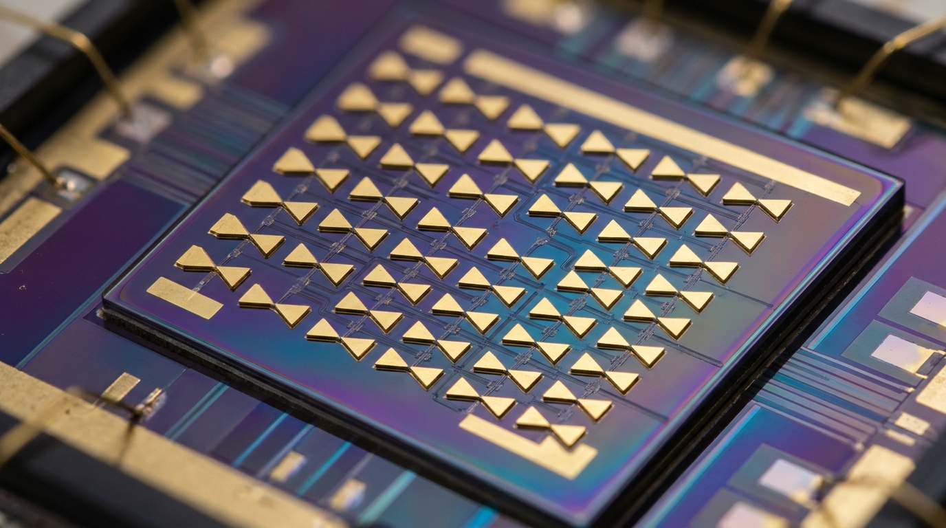
To establish durable ohmic connections and simultaneously mitigate series resistance, the team structured the underlying graphene beneath the antenna metallization and output contact pads with densely packed triangular holes possessing side lengths of 560 nanometers. This dense geometric patterning maximized the perimeter of metal-graphene edge contacts, thereby markedly lowering contact resistivity. Titanium and gold metal layers of five and thirty-five nanometers thickness were subsequently deposited by electron-beam evaporation to form the integrated 150-micrometer-long bowtie antennas featuring 60-degree flare angles. The final layout incorporated either isolated single-funnel channels or triple-funnel parallel arrangements, where tilted source and drain input arms inject carriers into an asymmetric stem to direct current toward a lower collection terminal rather than an opposing upper terminal.
Direct-current characterization across four-terminal devices confirmed that device transport occurs in the quasi-ballistic regime, where carrier mean free paths approach the physical width of the asymmetric constrictions. Transfer-length measurements under electrostatic gate sweeps revealed a room-temperature hole mobility of 3464 square centimeters per volt-second at zero gate bias, aligning with wafer-scale chemical vapor deposition standards, alongside an electron mobility of 2218 square centimeters per volt-second at ten volts gate bias. The corresponding maximum calculated mean free path reached approximately 65 nanometers for holes and 35 nanometers for electrons, directly comparable to the sub-100-nanometer constriction dimensions. Without applied gate bias, the hole mean free path stabilized near 60 nanometers, ensuring that carrier deflection at geometric boundaries dominates over bulk diffusive scattering within the channel.
Current-voltage characteristics recorded across the source and drain terminals exhibited distinct parabolic output profiles centered symmetrically around zero current bias, consistent with Landauer-Büttiker ballistic transport formalisms. Second-derivative analysis demonstrated that the quadratic curvature parameter reversed polarity across the charge neutrality point, confirming that rectification polarity follows the dominant majority carrier type rather than parasitic work-function offsets. Cryogenic measurements conducted at 20 Kelvin revealed an amplified quadratic curvature and elevated output magnitudes for both carrier polarities. Because thermoelectric Seebeck voltages and bolometric channel heating diminish substantially at reduced temperatures and oppose the observed polarity, these thermal side-effects were rigorously ruled out as dominant mechanisms, confirming that geometric asymmetry dictates the rectifying behavior.
High-frequency free-space optical characterization evaluated the rectenna prototypes under unguided, ambient conditions spanning 0.49 to 0.68 terahertz, driven by an electronically modulated synthesizer coupled to a frequency-multiplier source. A calibrated pyroelectric detector established an average incident source beam power of 50 microwatts at the source flange. Polytetrafluoroethylene collimating optics and off-axis parabolic mirrors directed the terahertz radiation upward through a hyperhemispherical silicon lens directly into the polished underside of the carrier wafer, focusing the beam into a 650-micrometer spot at the planar antenna. Throughout these high-frequency experiments, zero direct-current bias voltage and zero gate bias were applied to the devices, ensuring that detected signals arose strictly from passive zero-threshold rectification of induced high-frequency alternating currents.
Comparing the single-funnel geometry against the parallel triple-funnel rectenna revealed a dramatic performance enhancement directly attributable to improved antenna coupling. The measured extrinsic voltage responsivity climbed from 0.21 volts per watt in the single-funnel design to 0.77 volts per watt in the triple-funnel structure. When calibrated against isotropic radiator normalization conventions, the peak intrinsic responsivity reached 11.8 volts per watt for the triple-funnel array compared to 3.3 volts per watt for the single channel. Across the entire observed band, the responsivity of the triple-funnel structure was on average 4.7 times greater, closely matching a theoretical fourfold increase in quasi-static coupling efficiency from 2.1 percent up to 7.4 percent calculated from the real antenna feed-point impedance and measured device input resistances.
The enhanced responsivity yielded an immediate reduction in the equivalent optical detection noise floor, which is dominated entirely by intrinsic Johnson-Nyquist thermal fluctuations due to the absence of direct-current bias currents and the orthogonal layout of the input and output terminals. The minimum thermal noise-equivalent power calculated without normalization dropped from 108.2 nanowatts per square-root hertz for the single rectifier down to 29.2 nanowatts per square-root hertz for the triple-funnel configuration. Under isotropic antenna normalization, the minimum thermal noise equivalent power reached 1.9 nanowatts per square-root hertz. Concurrently, short-circuit current responsivity measurements across frequencies agreed with the measured direct-current output resistance of 31.6 kilohms, validating consistent device operation across electrical regimes.
The authors noted that current operating limitations, including the maximum 0.68-terahertz measurement ceiling, were dictated by the power thresholds of the laboratory multiplier source rather than intrinsic device transit-time boundaries. Furthermore, while the prototypes demonstrate responsivities competitive with uncooled zero-bias detectors, overall power conversion efficiency in this small-signal low-power regime remains below one percent. Scaling up channel counts beyond three rectifiers will eventually encounter diminishing returns due to wider input feed lines, non-uniform current injection, and parasitic channel-to-channel capacitive coupling. Nevertheless, by demonstrating reproducible device fabrication across separate wafers and highlighting compatibility with high-throughput nanoimprint lithography, this study demonstrates a viable pathway toward monolithically integrated zero-bias terahertz energy harvesters capable of powering autonomous sensors in emerging sixth-generation wireless networks.
Subject of Research: Terahertz geometric rectennas based on scalable chemical vapor deposition graphene for zero-bias energy harvesting
Article Title: Enhanced coupling efficiency in geometric terahertz rectennas based on scalable CVD graphene
Article References: Hemmetter, A., Holstein, J., Möller, M., Bolten, J., Canto, B., Ehlert, L., Ginzburg, A., Truccolo, D., Mencarelli, D., Midrio, M., Pierantoni, L., Lisauskas, A., Roskos, H., Wang, Z., & Lemme, M. C. (2026). Enhanced coupling efficiency in geometric terahertz rectennas based on scalable CVD graphene. Discover Electronics, 3(1), Article 128. https://doi.org/10.1007/s44291-026-00280-1
Image Credits: AI Generated
DOI: 10.1007/s44291-026-00280-1
Keywords: terahertz radiation, rectenna, graphene, chemical vapor deposition, geometric rectifier, zero-bias detection, energy harvesting, Internet of Things, 6G networks, ballistic transport, coupling efficiency, impedance matching, bowtie antenna, nanoelectronics, responsivity, noise equivalent power
News Source: Neil Sanderson. (November 13, 2026). Parallel Geometric Graphene Rectennas Boost Zero-Bias Terahertz Energy Harvesting. Scienmag.