


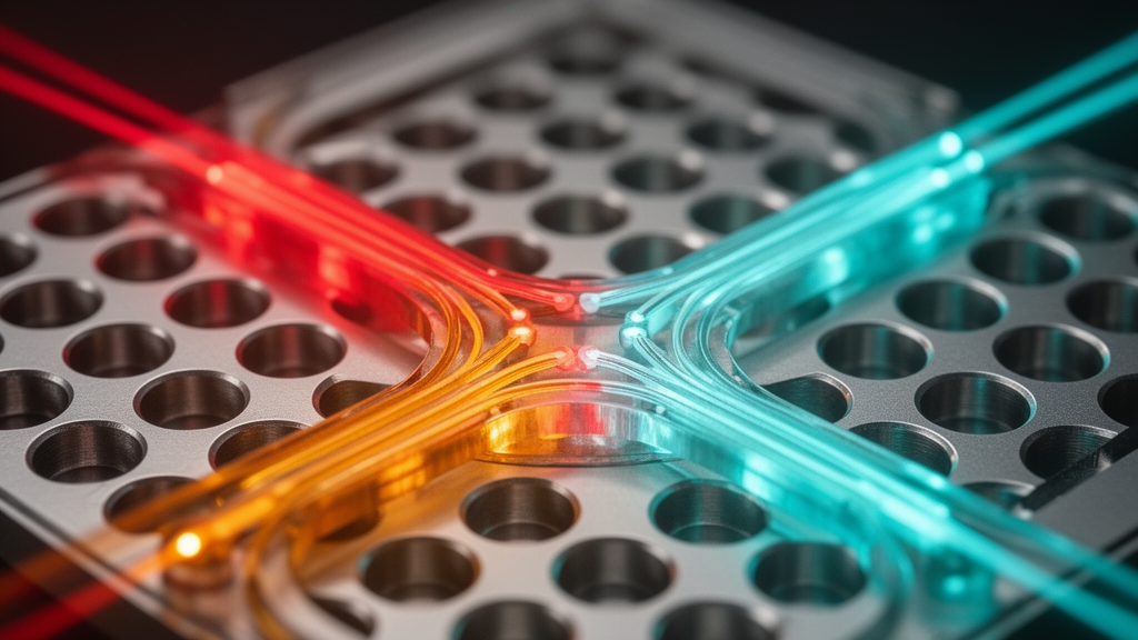
Optical communication architectures achieve high transmission speeds and broad bandwidths across long-distance networks, yet conventional signal processing relies extensively on electronic switches and routers. This recurrent conversion between optical and electronic signals introduces latency, increases electrical power consumption, and restricts the throughput of high-capacity data channels. To mitigate these bottlenecks, researchers have increasingly investigated all-optical data processing devices, such as optical logic gates and multiplexers, that manipulate, guide, and combine data streams entirely within the optical domain without electronic conversion. Operating entirely with light reduces energy dissipation and processing delays, facilitating higher overall operational efficiency in integrated optical circuits.
Photonic crystals provide an advantageous structural framework for compact optical computing due to their periodic distribution of refractive indices, which enables precise control and confinement of light at the nanoscale. These materials offer notable benefits, including wide operational bandwidths, compact physical dimensions, rapid response times, and straightforward potential for integration within integrated photonic circuits. Beyond standard photonic crystal configurations, related structures such as photonic crystal fibers have demonstrated strong light confinement for chemical and biochemical sensing applications. However, developing an all-optical two-by-one multiplexer that combines compact physical dimensions, high operating speeds, an acceptable contrast ratio, and dependable operational stability across shifting thermal environments has remained an ongoing engineering challenge.
To address these requirements, researchers Rashid Mozafari, Abdulhamid Zahedi, and Fariborz Parandin developed and analyzed a linear two-dimensional photonic crystal multiplexer incorporating a single localized defect rod. The physical layout utilizes a square lattice array of silicon rods surrounded by an air background substrate. The lattice constant of the periodic structure is set to 0.6 micrometers, and the radius of each silicon rod is 0.12 micrometers. The refractive index of the background air is 1.0, whereas the silicon rods exhibit a refractive index of 3.46, creating a substantial refractive index contrast of 2.46. The complete computational layout consists of a grid measuring 21 by 15 rods, forming a remarkably compact footprint covering an area of 108 square micrometers.
The band structure and waveguiding properties of the periodic array were determined through numerical simulations using the RSoft Photonic Suite, which integrates frequency-domain and time-domain analysis modules. The team first employed the BandSOLVE module to perform Plane Wave Expansion calculations, solving Maxwell equations in the frequency domain for infinitely periodic dielectric structures according to Bloch theorem. Computing eight photonic bands along the high-symmetry directions of the first Brillouin zone revealed a complete photonic bandgap exclusively under transverse magnetic polarization. This transverse magnetic bandgap spans normalized frequencies from 0.28 to 0.42, corresponding to free-space wavelengths between 1.42 micrometers and 2.14 micrometers. Because the standard optical communication wavelength of 1550 nanometers falls comfortably within this range, light propagation outside the intentional waveguide channels is completely forbidden.
Electromagnetic wave propagation and temporal switching dynamics were subsequently characterized using the FullWAVE solver, which implements the Finite Difference Time Domain technique. The continuous-wave optical source operated at 1550 nanometers, and the two-dimensional computational domain was discretized using standard Yee cells with a uniform spatial grid resolution of 0.01 micrometers in both directions, representing approximately 1/155 of the operating wavelength. Perfectly Matched Layer absorbing boundary conditions with a thickness of 0.5 micrometers were applied to eliminate unwanted edge reflections. The temporal discretization step was set to 0.0129, well below the Courant numerical stability limit of 0.0265, and simulations ran for 600 time units to ensure that all transient oscillations decayed and steady-state transmission was achieved.
The structural geometry of the multiplexer was created by selectively removing specific rows of silicon rods to establish three distinct input waveguide channels corresponding to input signals A, B, and the control select signal S, along with a single combined output waveguide channel. To optimize optical field confinement, coupling efficiency, and destructive interference, a specialized defect rod designated as R1 with a tailored radius of 48 nanometers was positioned at the center of the output waveguide. Coherent optical interference governs device functionality, requiring precise relative phase adjustments among the input sources. Preliminary parametric calculations established that setting the phase of input B to negative 40 degrees and the phase of the select signal S to negative 90 degrees produced optimal constructive and destructive interference, maximizing the distinction between logical high and logical low transmission states.
The multiplexer was evaluated across all eight possible binary input combinations to confirm complete logic functionality. In the baseline off state where inputs A, B, and S are inactive, no power exits the output waveguide, yielding an ideal off state with infinite insertion loss. When input B is activated alone, approximately 0.22 to 0.23 of the normalized input power reaches the output, which is interpreted as a logical zero with an insertion loss of 6.58 decibels. When only input A is active, the majority of the optical power transmits through to the output, reaching 0.66 normalized power with an insertion loss of 1.80 decibels, representing a clear logical one. In the state where both A and B are active without select signal S, the combined power reaches approximately 0.90 to 0.92 of the source power, exhibiting an insertion loss of only 0.46 decibels.
When the control select signal S is engaged, the device shifts its routing behavior. Activating S alone produces an output power of 0.23 with an insertion loss of 6.38 decibels, representing a logical zero. When inputs B and S are simultaneously active, their relative phase difference allows mutual constructive reinforcement, yielding an output power of 0.66 and an insertion loss of 1.80 decibels, functioning as a logical one. Conversely, when inputs A and S are active while B remains off, destructive interference between the out-of-phase waves attenuates the signal, causing the normalized output power to drop to 0.18 to 0.20 with an insertion loss of 6.99 decibels, establishing a clear logical zero. When all three inputs are simultaneously active, the normalized output power reaches 0.66 with an insertion loss of 1.80 decibels, matching the logical one specification. Establishing an upper threshold of 0.23 for logical zero and a minimum threshold of 0.66 for logical one provides clean signal differentiation and yields a calculated contrast ratio of 4.5 decibels.
Temporal analysis of the proposed device indicated a transient response time of approximately 0.2 picoseconds, defined as the duration required for the optical output to reach 90 percent of its final steady-state value from an initial condition. Inversely proportional to this rapid response time, the theoretical maximum data transfer rate reached 2.5 terabits per second. Comparative performance evaluations against previously reported two-by-one photonic crystal multiplexers highlight the operational balance of the proposed design. While earlier designs reported lower data rates ranging from 0.78 to 1.60 terabits per second or required complex nonlinear materials and dozens of structural defect rods, the current design achieves 2.5 terabits per second and a peak transmission efficiency of 90 percent using linear silicon rods and only a single defect element within a 108 square micrometer footprint.
A critical contribution of the study is a detailed thermal stability analysis evaluated over ambient temperatures ranging from 15 degrees Celsius to 55 degrees Celsius, relative to a baseline characterization at 25 degrees Celsius. Because temperature variations alter the refractive index of silicon through thermo-optic effects, the optical path lengths and coupling conditions inside photonic crystals can shift. However, simulations incorporating these thermo-optic perturbations demonstrated minimal impact on overall transmission. Output power across all logical states exhibited minor fluctuations, with worst-case power deviations remaining below approximately 7 percent, and states 7 and 8 exhibiting tight stability within plus or minus 0.01 normalized power units, confirming functional resilience against realistic temperature swings.
To evaluate sensitivity to potential manufacturing imperfections, the researchers performed fabrication tolerance simulations by independently varying the lattice constant, the radius of defect rod R1, and its physical alignment. Sweeping the lattice constant between 592 nanometers and 608 nanometers demonstrated that the contrast ratio remained robust, despite minor degradation away from the optimal 600-nanometer dimension. Similarly, altering the defect rod radius across a span from 40 nanometers to 56 nanometers revealed that while 48 nanometers delivered peak performance, acceptable multiplexing functionality persisted across the entire range. Shifting the defect rod position laterally by plus or minus 10 nanometers from the center line of the output waveguide likewise resulted in only minor performance variations, confirming reasonable resilience to standard lithographic alignment errors.
Although the proposed multiplexer relies on standard silicon-on-insulator compatible fabrication processes, such as electron-beam lithography combined with reactive ion etching or inductively coupled plasma dry etching, the authors noted that current findings remain confined to numerical simulations. The present work was restricted to a two-by-one multiplexing architecture, and experimental realization with physical grating couplers and physical power measurements was beyond the study’s scope. The authors stated that subsequent investigations will focus on experimental device fabrication, physical verification, and extending the linear design principles to higher-order optical multiplexing architectures while preserving rapid response times and thermal stability.
Subject of Research: Numerical design and simulation of a two-dimensional photonic crystal 2×1 all-optical multiplexer
Article Title: Design and simulation of a 2 × 1 optical multiplexer based on two-dimensional photonic crystals
Article References: Mozafari, R., Zahedi, A., & Parandin, F. (2026). Design and simulation of a 2 × 1 optical multiplexer based on two-dimensional photonic crystals. Results in Optics, Article 101202. https://doi.org/10.1016/j.rio.2026.101202
Image Credits: AI Generated
DOI: 10.1016/j.rio.2026.101202
Keywords: photonic crystals, optical multiplexer, integrated optics, finite difference time domain, plane wave expansion, silicon photonics, thermal stability, optical communication, optical logic circuits, contrast ratio, insertion loss, waveguides, defect engineering, terabit processing, telecommunications
News Source: Denise Maddox. (November 12, 2026). Photonic Crystal Multiplexer Achieves 2.5 Terabits per Second in Numerical Simulations. Scienmag.