


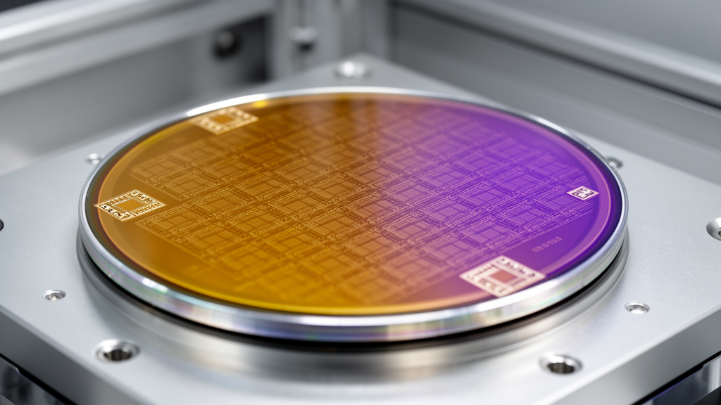
Researchers at the Graduate School of Engineering at The University of Tokyo, collaborating with institutions in Japan and Taiwan, have developed an atomically thin p-type semiconductor grown across an entire two-inch wafer. The experimental study, published in the journal Nature, details the synthesis of monolayer boron carbon nitride films and demonstrates high-performance field-effect transistors constructed from the material. By achieving continuous, single-layer crystal growth on copper substrates, the international research team has established a viable material platform that directly connects atomic-scale design with wafer-scale fabrication, offering a long-sought route toward scalable two-dimensional electronics.
Modern computing architectures depend fundamentally on complementary circuitry that combines both n-type transistors, which conduct electrical current via negatively charged electrons, and p-type transistors, which operate using positively charged holes. While two-dimensional semiconductors with high-performance n-type transport characteristics have progressed rapidly in recent years, comparable p-type materials capable of uniform synthesis across large surface areas have remained critically scarce. This persistent technological disparity has created a substantial bottleneck for the realization of energy-efficient complementary two-dimensional integrated circuits, making large-area p-type synthesis an essential milestone for the field.
To overcome this material barrier, the researchers focused on boron nitride, an atomically thin material comprising an ordered hexagonal network of alternating boron and nitrogen atoms that functions naturally as an electrical insulator. Drawing inspiration from conventional silicon semiconductor processing, where substitutional doping modifies electrical conductivity, the team introduced carbon atoms directly into the insulating hexagonal lattice during growth. Spectroscopic investigations confirmed that this targeted structural modification transforms the insulating framework into an active semiconductor featuring an electronic bandgap of approximately 1.90 electron volts. Atomic-resolution microscopy demonstrated that the resulting crystal lattice remains continuous despite local structural distortions, with carbon atoms and carbon pairs preferentially substituting for nitrogen positions within the analyzed regions.
The realization of continuous monolayer boron carbon nitride across a two-inch wafer required solving an intricate chemical delivery problem during epitaxial synthesis on copper (111) surfaces. In conventional synthesis attempts, a primary obstacle has been the spatial and temporal mismatch in supplying boron, carbon, and nitrogen chemical species simultaneously to the reactive growth front. To resolve this imbalance, the team utilized two molecular precursors: monomethyl ammonia borane and ammonia borane. By engineering their dehydrogenation and surface-reaction pathways, the researchers achieved coordinated delivery across the substrate, which effectively suppressed the formation of undesirable carbon-rich aggregates and favored clean carbon incorporation into the hexagonal boron nitride lattice.
The ability to manipulate material composition at the atomic level while maintaining large-scale structural coherence represents a central conceptual breakthrough of the project. Vincent Tung, a corresponding author of the study from The University of Tokyo, emphasized that controlling the precise insertion of carbon atoms into the host lattice allows the team to engineer electronic characteristics from the atomic scale upward. Tung noted that this chemical approach enables efficient electrical conduction while preserving the crystalline order necessary for reliable device operation. He further pointed out that the work proves atomic-level structural engineering and wafer-scale synthesis can proceed in tandem rather than presenting mutually exclusive processing demands.
To rigorously assess the electrical quality, uniformity, and manufacturing reproducibility of the synthesized material, the researchers fabricated and evaluated 224 boron carbon nitride field-effect transistors sourced across three independent growth batches. These p-type devices exhibited a field-effect hole mobility of approximately 100 square centimeters per volt-second alongside an on-state current exceeding 0.9 milliamperes per micrometer of channel width. Furthermore, the devices achieved an on/off current switching ratio of approximately 10⁸. The consistent statistical distribution of these electrical metrics across the entire two-inch wafer surface and between distinct processing runs verified the operational uniformity of the epitaxial growth method.
The experimental results establish that wafer-scale boron carbon nitride possesses the electrical and structural properties needed to complement advanced n-type two-dimensional semiconductors, although the researchers caution that a fully integrated complementary circuit has not yet been demonstrated. In addition to serving planar architectures, the thin profile and stability of the material offer potential pathways for future monolithic three-dimensional circuit integration. The team has outlined subsequent research objectives that center on sharpening atomic control over carbon substitution sites, reducing processing growth temperatures, demonstrating direct device-level integration with n-type channels, and maturing the chemical vapor synthesis into manufacturing-ready semiconductor workflows.
Subject of Research: Wafer-scale synthesis and transistor performance of monolayer p-type boron carbon nitride
Article Title: Carbon engineering turns insulating boron nitride into a wafer-scale p-type semiconductor
Article References: Carbon engineering turns insulating boron nitride into a wafer-scale p-type semiconductor. Original publication (Bibliographic details unavailable.)
Image Credits: AI Generated
DOI: Not provided
Keywords: Boron carbon nitride, Boron nitride, Two-dimensional semiconductors, P-type semiconductors, Wafer-scale synthesis, Field-effect transistors, Monolayer materials, Hexagonal boron nitride, Copper substrate, Substitutional doping, Hole mobility, Ammonia borane, Monomethyl ammonia borane, Electronic bandgap, Complementary electronics, Monolithic 3D integration, Epitaxial growth
News Source: Bethany Barker. (November 10, 2026). Wafer-Scale Boron Carbon Nitride Yields High-Performance P-Type Semiconductor Transistors. Scienmag.