


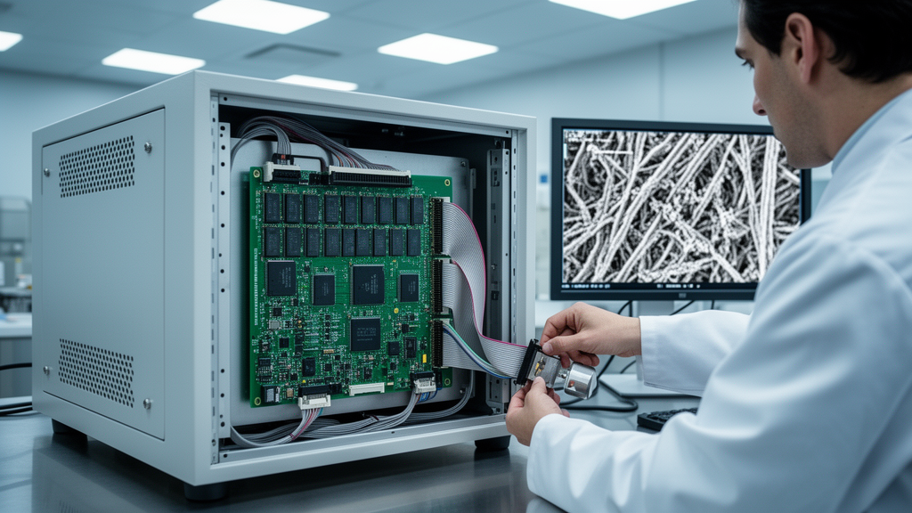
Scanning electron microscopes are among the most versatile imaging tools in modern science, but their performance depends heavily on electronics that most users never see: the circuits that sweep the electron beam across a specimen and digitize the faint signals that come back. In a quantitative benchmark, the custom electronics achieved spatial signal-to-noise ratios 41 to 47 percent higher than the instrument’s commercial reference, while operating at one-third of the per-frame acquisition time.
The system, described in the journal Applied Microscopy, was developed by Kyubin Gong, Junseok Kim, Bog G. Kim and Boklae Cho. At its heart sits a Xilinx Artix-7 FPGA (model XC7A35T), a reconfigurable logic chip that orchestrates every timing-critical function of the microscope’s scan-and-read cycle on a single device. Because the raster scan waveform generation, detector signal digitization and USB data streaming all run inside one common clock domain, the alignment between the beam’s position and the recorded pixel value is guaranteed at the hardware level rather than negotiated in software. That deterministic synchronization, the authors argue, is the key to the signal fidelity gains they report.
The hardware is organized into four functional blocks. A dual-channel AD9235 analog-to-digital converter with 12-bit resolution and a maximum sampling rate of 20 megasamples per second digitizes the secondary electron and backscattered electron signals simultaneously. On the output side, a dual-channel AD9767 digital-to-analog converter with 14-bit resolution and a 125 megasample-per-second update rate synthesizes the X and Y raster waveforms that drive the external scan-coil amplifiers. Communication is handled primarily by an FT232HL-based USB 2.0 High-Speed interface supporting sustained throughput of up to 40 megabytes per second, with Gigabit Ethernet provisioned for remote control and a UART link reserved for debugging and low-speed commands.
The physical implementation reflects careful analog engineering. The ADC and DAC expansion board measures 145 by 100 millimeters and uses a four-layer stack-up, with the analog conversion section physically partitioned from the digital control section to keep switching noise out of the signal path. The ADC input carries an anti-aliasing low-pass filter, the DAC output includes a reconstruction filter, and high-speed data lines are routed to a 100-ohm differential impedance target while clock lines target 50 ohms single-ended, minimizing jitter and ground bounce. Analog and digital power rails are separated, and bypass capacitors sit at every integrated circuit power pin. The board was fabricated and assembled by JLCPCB and connects to an AX7035B FPGA development board through a 40-pin expansion connector.
The firmware is equally modular, written as independent Verilog HDL modules for command parsing, scan waveform generation, data acquisition and communication, all integrated in a top-level design file. Commands arriving over UART are checked against a fixed-length packet protocol with a header, command code, parameter field and terminator; only frames passing integrity verification update the internal register file. That allows scan resolution, oversampling factor, scan rate and scan mode to be reconfigured mid-experiment without halting the system. The waveform generator supports scan resolutions from 512 by 512 up to 4,096 by 4,096 pixels, extendable to 16,384 by 16,384 scan points by widening internal register widths, and real-time on-chip averaging accumulates 50 clock cycles of samples per scan point before the data enter FIFO memory for interleaved streaming.
Bench verification confirmed the design intent. An oscilloscope recorded the DAC-generated sawtooth waveform at approximately 961 hertz, matching the line-scan rate calculated from the configured parameters, and Lissajous displays of the X and Y signals confirmed stable phase alignment between the fast-scan and slow-scan axes. A programmable retrace parameter accelerates the flyback portion of each scan line, reducing the fraction of frame time lost to repositioning. Injecting distinct test ramp and staircase signals into the two ADC channels verified that both were digitized in full temporal synchronization through the odd-even interleaving scheme that merges the channels into a single stream.
The team then integrated the module into a commercial ModuleSci PicoEye-100 SEM, connecting the DAC outputs directly to the deflection electronics and the ADC inputs to the secondary electron detector preamplifier. In the fast-scan mode routinely used for alignment and focusing, with roughly one second per frame at 1,024 by 1,024 pixels, the system produced clearly resolved secondary electron images of a calibration grid with a 125 micrometer pitch at magnifications of 2,500 and 6,000 times. Mild geometric distortion near the image boundaries, attributed to settling behavior of the scan-coil driver during flyback, remains an acknowledged limitation, and the images were acquired without orthogonality correction or scale calibration.
The quantitative benchmark was conducted separately under standard acquisition conditions, at 10 seconds per frame, on the same microscope held at identical column settings: 20.0 kilovolts accelerating voltage, 8.0 millimeter working distance and spot-size setting 7, imaging a copper calibration mesh at 10,000 times magnification. The FPGA system acquired 10-second frames averaged offline over groups of 1, 4, 9, 16 and 25 frames, while the commercial reference acquired a single 30-second frame at a slower scan speed. An identical four-step processing pipeline was applied to both datasets: grid-hole masking to exclude vacuum regions, histogram normalization to remove format-related noise-floor bias from the JPEG output of the commercial channel, sub-pixel drift correction using the cross-correlation method of Guizar-Sicairos and colleagues, and frame averaging.
The results were striking. Beyond the 41 to 47 percent spatial SNR advantage, temporal SNR followed the theoretically expected square-root-of-N scaling with an R-squared of 0.998 when sub-pixel drift correction was applied, reaching 27.5 at 25 averaged frames, a 4.98-fold improvement over the commercial reference, whose scaling efficiency suffered from residual misalignment. Without drift correction, standard alignment achieved only about 43 percent of the theoretical averaging gain. Resolution analysis after correcting for a 1.66-fold pixel-size difference showed that from four frames onward the FPGA system achieved a smaller edge FWHM of 56.1 nanometers, 22 percent below the commercial reference’s 71.9 nanometers, and higher MTF50 values of 9.3 to 10.5 cycles per micrometer, 23 to 39 percent above the reference’s 7.58.
The authors are careful about what these resolution numbers mean. The intrinsic electron-optical resolution of the SEM is governed by the column itself and is independent of the acquisition electronics, so the narrower FWHM and higher MTF50 should be read not as a change in the microscope’s inherent resolving power but as more reliable practical recovery of high-frequency spatial detail that the column already delivers, enabled by higher SNR and stable averaging. Validation so far covers a single SEM platform, and the team notes that scan linearity and orthogonality correction are not yet fully implemented. Future work targets real-time geometric correction, multi-channel acquisition and higher-throughput interfaces. Because the architecture consolidates scan generation and synchronized acquisition in one low-cost module, the researchers suggest it could serve point-scanning instruments well beyond electron microscopy, from confocal microscopes to ultrasonic and eddy-current inspection systems.
Subject of Research: An FPGA-based reconfigurable scanning and data acquisition system that improves signal-to-noise performance in scanning electron microscopy
Article Title: FPGA-based reconfigurable scanning and data acquisition system for scanning electron microscopy
Article References: Gong, K., Kim, J., Kim, B. G., & Cho, B. (2026). FPGA-based reconfigurable scanning and data acquisition system for scanning electron microscopy. Applied Microscopy, 56(1), Article 16. https://doi.org/10.1186/s42649-026-00137-7
Image Credits: AI Generated
DOI: 10.1186/s42649-026-00137-7
Keywords: scanning electron microscopy, FPGA, data acquisition, signal-to-noise ratio, raster scanning, Xilinx Artix-7, image quality, drift correction, MTF, hardware synchronization, electron microscopy instrumentation, FPGA-based
News Source: Denise Maddox. (October 29, 2026). Custom FPGA Electronics Boost SEM Image Signal-to-Noise by Up to 47 Percent. Scienmag.