


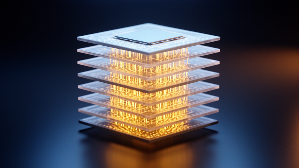
Dynamic random-access memory has long advanced by shrinking cells onto flat, two-dimensional wafers, but a new review argues that this approach is running out of room. According to a Review article published in Nature Reviews Electrical Engineering, moving to sub-10-nanometre process nodes raises serious concerns about the scalability and long-term viability of conventional 2D DRAM architectures, and the authors make the case that cell-stacked three-dimensional DRAM is the most credible route forward.
The review, led by Joon Young Kang and Cheol Seong Hwang with colleagues, traces the evolution of 2D DRAM and identifies the specific bottlenecks that now constrain it. As cells shrink below the 10-nanometre mark, capacitor scaling becomes increasingly difficult, word-line resistance rises, and cell-to-cell interference grows more troublesome. The authors also highlight the row-hammer effect, a well-known reliability problem in dense DRAM arrays, as one of the challenges facing continued two-dimensional scaling.
The proposed solution is distinct from chip-stacked high-bandwidth memory, the approach already used in some advanced computing products. Instead of stacking complete memory chips on top of one another, cell-stacked 3D DRAM would integrate the memory cells themselves in a vertical arrangement, allowing bit density to grow in the third dimension rather than in the plane of the wafer.
One of the review’s key quantitative claims concerns when this transition becomes worthwhile. The authors calculate that cell-stacked 3D DRAM can surpass the bit density of 2D DRAM at approximately 100 stacked layers, providing a scalable path beyond planar architectures.
Realizing such a memory will require more than simply turning existing structures on their side. The review identifies circuit and structural innovations as prerequisites, including vertical bit-line designs, gate-all-around transistors, and new channel materials. Among those materials, single-crystal silicon remains the leading candidate, while amorphous oxide semiconductors such as indium gallium zinc oxide are emerging as promising alternatives for future 3D DRAM devices.
The vertical bit-line architecture carries a particularly concrete benefit. According to the review, it can reduce bit-line capacitance by approximately threefold compared with horizontal bit-line designs, which improves sensing scalability.
The authors are candid about the obstacles that remain. Process integration challenges, including the fabrication of staircase word-line contacts and wafer bonding, currently hinder the realization of scaled 3D DRAM. High aspect-ratio fabrication, interconnect design and long-term reliability are also listed among the key challenges that must be solved before practical stacked memory can reach production.
Despite these hurdles, the review’s overall assessment is optimistic. As a review article, the work synthesizes existing research and outlines a development roadmap rather than reporting a new experimental device, but it frames the coming architectural transition in unusually concrete terms: the planar era of DRAM is nearing its limits, and the vertical era is the planned successor.
Subject of Research: Three-dimensional stacked DRAM as a successor to scaled two-dimensional DRAM architectures
Article Title: Three-dimensional dynamic random-access memory beyond two-dimensional scaling limits
Article References: Kang, J. Y., Choi, J., Shin, J., Song, H., Park, T. W., Han, J.-W., Ha, D., Kim, J. J., & Hwang, C. S. (2026). Three-dimensional dynamic random-access memory beyond two-dimensional scaling limits. Nature Reviews Electrical Engineering. https://doi.org/10.1038/s44287-026-00347-x
Image Credits: AI Generated
DOI: 10.1038/s44287-026-00347-x
Keywords: DRAM, 3D memory, semiconductor scaling, vertical bit line, gate-all-around transistors, oxide semiconductors, wafer bonding, memory architecture, artificial intelligence computing, row hammer, capacitor scaling, high aspect-ratio fabrication
News Source: Denise Maddox. (October 27, 2026). Stacked 3D DRAM offers a path beyond two-dimensional scaling limits. Scienmag.