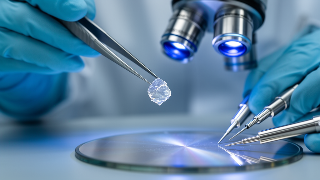
In a result that could reshape how the electronics industry approaches the atomic-scale limits of silicon, researchers in South Korea have transformed a single layered crystal into a complete, working transistor without ever assembling the device from separate parts. The team, led by Director Jo Moon-Ho of the Center for Van der Waals Quantum Solids at the Institute for Basic Science, demonstrated that one atomically thin crystal of tungsten diselenide can be chemically converted, region by region and layer by layer, into every functional component a modern transistor requires: a semiconducting channel, an insulating gate dielectric, and low-resistance electrical contacts. The work, published in the journal Science, points toward a future in which entire electronic devices are carved out of a single parent material rather than stitched together from incompatible pieces.
The challenge the researchers set out to solve is one of the most stubborn in condensed matter physics and device engineering. A conventional transistor is not made of one material but of several fundamentally different ones working in intimate contact. A semiconductor carries the current, a dielectric insulator controls it through an applied gate voltage, and metallic or semimetallic contacts allow charge to enter and exit. As silicon devices shrink toward their physical scaling limits, atomically thin two-dimensional semiconductors have been heralded as natural successors. Yet for more than two decades, the obstacle to practical 2D electronics has rarely been the performance of the semiconductor itself. It has been the integration problem: how to attach the other components without destroying the delicate atomic sheet they must sit upon.
The surfaces of two-dimensional semiconductors are chemically inert in a troublesome way. They contain few dangling bonds or reactive sites where other materials can anchor, which makes it extraordinarily difficult to deposit a gate dielectric uniformly across them. Conventional dielectric deposition tends to produce patchy, leaky films on such surfaces. Direct metal deposition is equally problematic, since the energetic process can damage the atomically thin semiconductor or create large contact barriers that choke off the flow of charge. Mechanical transfer methods, in which separate 2D materials are peeled, aligned, and stacked one by one, offer an alternative, but they are slow, difficult to scale uniformly over large areas, and poorly suited to the demands of mass production.
The IBS team’s answer was to stop thinking of the crystal as just the semiconductor and start treating it as the raw material for everything. They began with multilayer tungsten diselenide, a two-dimensional semiconductor whose electrical character can be altered by replacing the atoms surrounding the tungsten layer. By preserving the tungsten framework while selectively swapping those surrounding atoms, the researchers changed the electronic identity of individual regions without rebuilding the crystal from scratch. The upper layers were first oxidized into insulating tungsten oxide, and that oxide could then be further converted through vapor-phase reactions into either tungsten disulfide, an n-type semiconductor, or tungsten ditelluride, a semimetal. Regions left untouched retained the original tungsten diselenide semiconductor behavior. In this way, semiconducting, insulating, and semimetallic functions were created directly within different layers and locations of the same parent crystal.
The precision of the method rests on a remarkably elegant physical principle: the tiny gaps between neighboring atomic layers act as natural barriers that confine the chemical reaction. By tuning the reaction temperature and gas pressure, the researchers could halt the conversion after a chosen number of layers, achieving depth control of roughly 0.7 nanometers per tungsten diselenide monolayer. That is the thickness of a single atomic sheet, meaning the process can be steered with a resolution measured in individual atomic planes. This layer-by-layer chalcogen substitution, as the technique is known, effectively turns a crystal-growth problem into a controllable chemical editing problem, one atomic layer at a time.
The most consequential demonstration involved converting the upper layers of tungsten diselenide into tungsten oxide directly above the semiconductor channel. The resulting oxide served as the gate dielectric without any need to deposit a separate high-permittivity material, forming an insulating layer with an effective thickness below one nanometer while maintaining strong insulating performance. This is a significant achievement, because the gate dielectric is where many would-be 2D devices fail. A dielectric that is too thick or too leaky wastes voltage and allows current to slip through when the transistor should be off. A dielectric grown from the channel material itself, atom-for-atom matched to the surface beneath it, sidesteps the interface problems that have plagued conventional deposition.
The electrical performance of the resulting devices came astonishingly close to theoretical ideals. Using this self-grown oxide, the researchers fabricated tungsten diselenide transistors in which a change of only 61.3 millivolts in gate voltage increased the current tenfold. That figure sits very near the theoretical room-temperature limit of about 60 millivolts per decade, the so-called Boltzmann limit that defines the most efficient switching any conventional transistor can achieve. The devices also achieved an on/off current ratio exceeding ten million, meaning the difference between the transistor’s conducting and blocking states spans more than seven orders of magnitude. For low-power electronics, where every wasted millivolt translates into wasted energy, these numbers represent the kind of switching efficiency that device engineers spend careers pursuing.
The contact side of the problem was addressed with equal precision. When the upper layers were converted into tungsten ditelluride, a semimetal, the resulting contacts reduced the barrier for charge injection to about one-third of what was observed with direct platinum contacts. Lower injection barriers mean charge carriers can enter the semiconductor more freely, cutting the parasitic resistance that has historically limited the performance of 2D transistors. The semimetal-to-semiconductor junction created by chemical conversion is also atomically clean by construction, since it forms within the same crystal lattice rather than across the boundary between two separately grown materials.
To show that the method extends beyond individual devices, the team fabricated n-type molybdenum disulfide transistors using the same tungsten oxide dielectric, and then stacked p-type and n-type transistors vertically to construct a complementary van der Waals inverter, a basic building block of digital logic. The successful voltage inversion demonstrated that the technique is not merely a laboratory curiosity for single transistors but a plausible foundation for more highly integrated circuitry. Vertical stacking of complementary devices is particularly attractive for future electronics, because it multiplies functional density without shrinking lateral dimensions further, a direction the industry finds increasingly costly.
The implications reach well beyond one material system. The study combines fundamental materials science based on atomic-scale manipulation with modern semiconductor technology, addressing what Jo Moon-Ho described as the central integration challenge in two-dimensional semiconductor research: not simply finding better semiconductors, but securing equally suitable dielectrics and electrical contacts. By directly converting selected regions of a two-dimensional crystal into different electronic functions, the approach could provide a new route toward ultralow-power, ultrascaled, and vertically integrated semiconductor devices. If the method can be scaled to wafer dimensions with the same layer-by-layer precision demonstrated here, the era in which a complete transistor is grown rather than assembled may be closer than the industry dared expect.
Subject of Research: Layer-by-layer chemical conversion of a single 2D crystal into semiconducting, insulating, and semimetallic regions for integrated transistors
Article Title: Turning single 2D crystal into a complete high-performance transistor
Article References: Turning single 2D crystal into a complete high-performance transistor. (n.d.). Original publication
Image Credits: AI Generated
DOI: Not provided
Keywords: two-dimensional materials, tungsten diselenide, transistors, gate dielectric, chalcogen substitution, van der Waals heterostructures, semiconductors, tungsten ditelluride, low-power electronics, integrated circuits, Institute for Basic Science, atomic-scale fabrication
News Source: Denise Maddox. (October 16, 2026). Scientists Turn a Single 2D Crystal Into a Complete High-Performance Transistor. Scienmag.