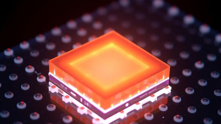
Silicon has ruled the worlds of solar energy and light sensing for decades, but the humble element may have just received a remarkable upgrade. Researchers report that a cleverly engineered polymer interlayer, built from nothing more exotic than repeated spin-coating of a common conductive polymer, can boost the photocurrent of a silicon-perovskite photodetector by more than 170 times compared with a device lacking the interlayer. The work, published in the journal Results in Optics, demonstrates that careful control of an interface just a hundred nanometers thick can transform the performance of a hybrid light-sensing device fabricated entirely under ambient conditions.
The team, led by Zeinab PourMohammadi, Fatemeh Dehghan Nayeri, and Rouhollah Azimirad, focused on a heterojunction device that sandwiches the archetypal perovskite methylammonium lead iodide, known as MAPbI3, on top of p-type silicon. Silicon remains the backbone of the photovoltaic and optoelectronic markets thanks to its abundance, stability, and excellent electronic properties, but forming traditional silicon junctions requires high-temperature doping processes and sophisticated equipment. Pairing silicon with metal halide perovskites offers a cheaper, low-temperature alternative. MAPbI3, a crystalline material with the general ABX3 perovskite formula, brings direct-bandgap light absorption, low exciton binding energy, long carrier diffusion lengths, and simple solution processing to the partnership. In principle, the combination should harness the best of both materials.
In practice, however, the marriage has a persistent flaw. When silicon and perovskite are pressed directly against each other, mismatched energy band alignment creates a poor electrical contact. Photoexcited charge carriers recombine at the interface before they can be collected, squandering the very light the device is meant to detect. The standard remedy is a buffer layer, a thin film that bridges the two dissimilar materials and smooths out the energetic landscape. Previous studies have tested metal oxides such as tin dioxide, gallium oxide, and titanium dioxide in this role, each with its own trade-offs between dark current, recombination, and tunneling efficiency.
The new study takes a different route by turning to PEDOT:PSS, the workhorse hole-transport polymer of the perovskite world. This material is a polymer electrolyte with a split personality: positively charged PEDOT is highly conductive but water-insoluble, while negatively charged PSS is insulating but acts as a surfactant that lets PEDOT disperse in water. The two components naturally form a micelle-like structure, with conductive PEDOT cores wrapped in nonconductive PSS shells. Crucially for the new work, the arrangement of these components is not fixed. During spin-coating, the denser, hydrophobic PEDOT phase settles toward the bottom of the film while the hydrophilic PSS-rich phase accumulates at the surface, and a mild 120-degree-Celsius bake does not remix them.
The researchers exploited this segregation with an elegantly simple modification: instead of depositing a single PEDOT:PSS layer spun at 2000 rpm, they applied two consecutive coatings, first at 1500 rpm and then at 2000 rpm, with no chemical additives of any kind. Each new spin-coating cycle exposes the PSS-rich surface to water, which partially washes it away and replaces it with the conductive PEDOT-rich phase. With every additional layer, the stack becomes richer in PEDOT at the bottom and leaner in insulating PSS, driving down sheet resistance without a proportional increase in thickness. The resulting bilayer measured about 100 nanometers total, barely thicker than the roughly 90-nanometer single layer, yet its conductivity was inferred to be substantially higher.
The benefits rippled far beyond simple conductivity. Scanning electron microscopy revealed that perovskite films grown on the modified bilayer contained far fewer pinholes than films grown on pristine PEDOT:PSS, which itself performed worse than bare silicon in this respect. The explanation lies in surface physics: multiple coatings increase the roughness of the polymer layer, and according to the Wenzel equation, roughness enhances wettability. Better wetting lowers the energy barrier for perovskite nucleation, creating more nucleation sites and a more complete, pinhole-free film. Pinholes matter enormously because they introduce trap states and shunt paths that degrade carrier lifetime and cause leakage, so suppressing them directly improves device quality.
Structural analysis told a consistent story. X-ray diffraction confirmed the tetragonal MAPbI3 phase in all samples, with the characteristic (110) preferred orientation, but films grown on PEDOT:PSS interlayers showed sharper peaks and larger crystallites. Using the Williamson-Hall method, the team extracted crystallite sizes of about 99 nanometers for films on both pristine and modified PEDOT:PSS, compared with only 55 nanometers for perovskite grown directly on silicon, which also carried a compressive microstrain. Larger grains mean fewer grain boundaries, less carrier scattering, and less recombination. Notably, the telltale diffraction peaks of residual lead iodide, prominent in the silicon-only sample, were strongly suppressed by the interlayer, suggesting the acidic polymer promotes complete conversion of precursors into the perovskite phase, a factor linked to better device stability.
Optical and electrical measurements sealed the case. Photoluminescence from the perovskite was strongly quenched on the interlayer samples, indicating efficient extraction of photoexcited carriers by the built-in electric field at the heterojunction, with the modified layer outperforming all alternatives. A blue shift in the emission peak further hinted at reduced trap density near the band edges. Under 530-nanometer laser illumination at a modest intensity of 0.3 milliwatts per square centimeter, all devices showed rectifying behavior from the built-in field, but the champion device with the modified interlayer delivered a photocurrent roughly 170 times greater than the interlayer-free control at a reverse bias of 5 volts. The device achieved a responsivity of 0.78 amperes per watt and a detectivity of 4.9 times ten to the eleventh Jones, figures that compare competitively with recent perovskite-based photodetectors, many of which required far more elaborate fabrication.
The authors are careful to frame the work as a proof of concept. Direct carrier-lifetime measurements were not performed, and long-term stability testing remains a key direction for future investigation, particularly because the hygroscopic nature of PEDOT:PSS is a known degradation risk for MAPbI3 devices. Even so, the bilayer design offers two plausible stability advantages: the reduced PSS content should make the polymer less hydrophilic, and the denser perovskite film should limit moisture ingress into the bulk. If those predictions hold up, the implications are significant. A photodetector that combines silicon’s maturity with perovskite’s optical prowess, assembled from solution at room temperature with a modification as simple as spinning the same material twice, points toward scalable, low-cost hybrid optoelectronics in which the trade-off between performance and processability is decisively rebalanced.
Subject of Research: Enhancement of silicon/MAPbI3 heterojunction photodetectors using a modified bilayer PEDOT:PSS interlayer
Article Title: Improving photodetection ability of Si/MAPbI 3 heterojunction by using modified PEDOT:PSS interlayer
Article References: PourMohammadi, Z., Nayeri, F. D., & Azimirad, R. (2026). Improving photodetection ability of Si/MAPbI3 heterojunction by using modified PEDOT:PSS interlayer. Results in Optics, Article 101177. https://doi.org/10.1016/j.rio.2026.101177
Image Credits: AI Generated
DOI: 10.1016/j.rio.2026.101177
Keywords: photodetector, perovskite, silicon, PEDOT:PSS, MAPbI3, heterojunction, interlayer, spin coating, responsivity, detectivity, thin films, optoelectronics
Cite Scienmag News
APA MLA Chicago
Neil Sanderson. (October 1, 2026). Simple Polymer Trick Boosts Silicon-Perovskite Photodetector Performance 170-Fold. Scienmag. https://scienmag.com/simple-polymer-trick-boosts-silicon-perovskite-photodetector-performance-170-fold/
Neil Sanderson. “Simple Polymer Trick Boosts Silicon-Perovskite Photodetector Performance 170-Fold.” Scienmag, 1 October 2026, https://scienmag.com/simple-polymer-trick-boosts-silicon-perovskite-photodetector-performance-170-fold/. Accessed 1 October 2026.
Neil Sanderson. “Simple Polymer Trick Boosts Silicon-Perovskite Photodetector Performance 170-Fold.” Scienmag. October 1, 2026. https://scienmag.com/simple-polymer-trick-boosts-silicon-perovskite-photodetector-performance-170-fold/
Copy citation Download RIS
Tags: ambient condition device fabricationconductive polymer spin-coatingdetectivityheterojunctionhybrid light-sensing deviceinterface engineering in optoelectronicsinterlayerlow-temperature perovskite fabricationMAPbI3nanometer-thick interface controlOptoelectronicsPEDOT:PSSperovskiteperovskite methylammonium lead iodidephotocurrent amplificationphotodetectorphotodetector performance improvementpolymer interlayer enhancementresponsivitysiliconsilicon-perovskite heterojunctionssilicon-perovskite photodetectorsspin coatingthin films