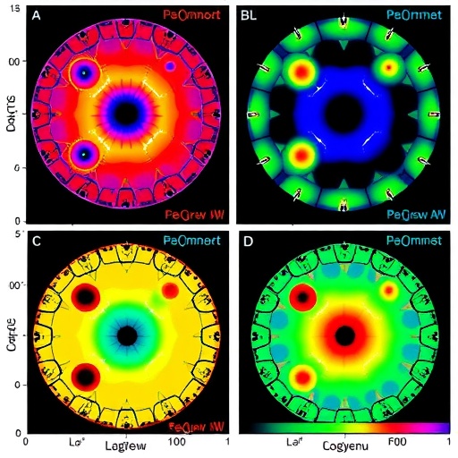
A team has mapped, in real time and with nanoscale precision, how photogenerated holes travel and react inside a facet-engineered bismuth vanadate photocatalyst. Using a home-built in-situ transient reflection microscope (TRM), the researchers visualized the full spatiotemporal pathway of these charge carriers at the solid–liquid interface—where photocatalysis often succeeds or fails.
The study tackles a central bottleneck in artificial photosynthesis: after light absorption, carriers must be separated, transported, and transferred to reactive sites. In many photocatalysts, these steps are slowed or rerouted by trapping at defects and by interfacial energy losses, ultimately reducing overall conversion efficiency.
While semiconductor carrier behavior has been widely investigated, directly tracking charge evolution on individual photocatalyst crystals under realistic reaction conditions has remained extremely difficult. By combining facet engineering with an optical measurement strategy tailored to transient carrier dynamics, the team overcame this challenge and followed holes as they evolved from formation to interfacial transfer.
Their observations reveal a three-stage sequence for photogenerated holes. First, charge separation occurs within about 5 picoseconds, setting the initial conditions for subsequent transport. Second, the holes become captured by defect states, with a characteristic trapping time of roughly 1.5 nanoseconds.
Third, the trapped holes are rapidly transferred to the interface with a time constant near 19 picoseconds. This interfacial step is mediated by oxygen-related defect structures, which act as functional conduits between the semiconductor interior and the surrounding liquid environment.
Crucially, the in-situ visualization clarifies what trapped holes actually do—rather than treating trapping as a purely harmful process. The results indicate that defect states can be integral to efficient oxidation by enabling timely hole availability at reactive interfaces.
Beyond shedding light on the fundamental mechanism, the work provides a framework for rational photocatalyst design. It suggests that defect engineering—optimizing both trapping and transfer pathways—can be a direct route to higher photocatalytic performance.
The findings were reported in a recent article in National Science Review, offering viral-science impact by converting a long-standing “black box” of carrier dynamics into a measurable, controllable sequence.
Subject of Research: Not applicable
Article Title: Unraveling the evolution of photogenerated holes from charge separation to interfacial transfer in photocatalysis
News Publication Date: 18-Jun-2026
Web References: https://doi.org/10.1093/nsr/nwag379
References: 10.1093/nsr/nwag379
Image Credits: DICP
Keywords
Catalysis; photocatalysis; carrier dynamics; transient reflection microscopy; defect engineering; charge separation; interfacial transfer; bismuth vanadate
Tags: charge separation and transfer mechanismscharge trapping and transfer timescalesdefect trapping in semiconductor photocatalystsfacet-engineered bismuth vanadate photocatalystin-situ transient reflection microscopyinterfacial energy losses in artificial photosynthesisnanoscale real-time charge carrier mappingnanoscale visualization of charge carrier pathwaysoptimization of photocatalyst efficiencyphotogenerated hole dynamics in photocatalysisphotogenerated hole evolution at solid-liquid interfaceultrafast charge separation processes