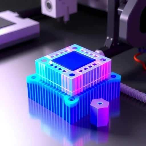
In a groundbreaking development poised to revolutionize the semiconductor industry, researchers at the Cockrell School of Engineering, University of Texas at Austin, have engineered a novel extreme ultraviolet (EUV) lithography printer. This innovation drastically reduces the size and cost of EUV lithography systems, traditionally massive and prohibitively expensive machines, thereby democratizing access for research institutions and smaller manufacturers. The new device’s compact, tabletop design integrates essential components stripped down to their core functionalities, setting a new standard in semiconductor fabrication technology.
The semiconductor manufacturing landscape traditionally hinges on EUV lithography, a technique instrumental in printing intricate circuits onto silicon substrates, forming the backbone of chips embedded in modern electronics such as smartphones, laptops, and an ever-expanding array of digital devices. EUV lithography depends on complex configurations involving precision mirrors, tin vapor light sources, and painstakingly crafted photomasks. However, available commercial EUV printers demand investments north of $200 million and occupy entire rooms, limiting their availability to only a handful of global corporations.
Responding to these challenges, the Texas engineering team, in collaboration with renowned research partners, embarked on reinventing the EUV lithography process. By reducing the architecture to its fundamental elements, they created a more versatile and modular system. This reimagined EUV printer is not only accessible to a broader range of users but opens new avenues for experimental modifications, accelerating developmental cycles in semiconductor research.
Beyond redesigning the hardware, the researchers merged this compact EUV device with an innovative lithographic technique: volumetric 3D patterning. Conventional EUV lithography processes are constrained to two-dimensional, layer-by-layer assembly of three-dimensional nanostructures, inherently slowing down production due to sequential exposure and alignment requirements. The volumetric 3D approach circumvents this barrier by enabling simultaneous patterning of multiple layers at once, cutting down exposure times from days to mere minutes without compromising nanoscale precision or feature complexity.
Chih-Hao Chang, a mechanical engineering professor and one of the lead authors of the study published in Nano Letters, highlights this transformative leap. He explains that although the pure printing duration might not be lengthy, the traditional repeated processing steps accumulate to prolonged fabrication times. Their volumetric method slashes this bottleneck, empowering researchers to prototype intricate 3D nanostructures rapidly, fostering innovation at an unprecedented pace.
This research represents a vital contribution to the National Science Foundation’s Future of Semiconductors (FuSe2) initiative, an ambitious program aimed at lowering the barriers and costs associated with semiconductor research. By creating practical, compact, and cost-effective EUV lithography systems, the Cockrell team supports the overarching goal of revitalizing semiconductor innovation and expanding participation beyond current industrial giants.
Currently, the team is actively testing novel EUV-sensitive materials developed collaboratively with UT Dallas and Johns Hopkins University, tailored specifically for their compact printer system. These material advances are crucial in optimizing the efficiency and resolution capabilities of the new fabrication platform, fine-tuning it to meet and potentially surpass existing industry standards.
Despite the exceptional promise, the researchers acknowledge that current limitations confine patterning to periodic nanostructures, primarily relevant for applications in photonics and memory chips. However, the long-term vision is ambitious: to engineer faster printers capable of crafting increasingly complex and smaller features, essential for the next generation of semiconductor switches. Such improvements directly translate into chips with enhanced computational power and energy efficiency.
Saurav Mohanty, a recent Ph.D. graduate and the study’s first author, envisages applications reaching far beyond the realm of semiconductors. He articulates that the ability to seamlessly pattern three-dimensional nanostructures could have tremendous impact in diverse fields including nanomedicine—for precise drug delivery systems—quantum computing architectures where nanoscale control is paramount, and the synthesis of novel materials with unique quantum or photonic properties.
This research is not merely an incremental update but a paradigm shift that redefines accessibility and scalability in semiconductor manufacturing. The miniaturization of EUV lithography equipment opens previously inaccessible experimentation avenues and democratizes a critical technology once monopolized by a select few. By enabling rapid and flexible nanofabrication, the Cockrell team’s innovation accelerates progress toward the pursuit of more powerful, efficient, and compact electronics.
As the semiconductor industry faces increasing pressures to sustain Moore’s Law and address the escalating costs of chip manufacturing, combining hardware innovation with advanced patterning strategies represents a holistic approach to overcoming these challenges. The future envisaged by these researchers includes faster prototyping periods, widespread experimental capabilities, and ultimately, the fabrication of semiconductor devices with unprecedented complexity and performance.
In conclusion, the work emerging from the Cockrell School of Engineering underscores the crucial interplay between mechanical engineering, materials science, and applied physics in pushing the boundaries of lithographic technology. The implications of this research resonate throughout the technology sector and beyond, promising to catalyze a wave of advancements not only in electronics but also in medicine, quantum sciences, and advanced material synthesis.
Subject of Research: Development of a compact and cost-effective extreme ultraviolet (EUV) lithography printer for rapid three-dimensional nanopatterning.
Article Title: Three-Dimensional Nanopatterning Using Extreme Ultraviolet Colloidal Talbot Lithography
Web References:
DOI: 10.1021/acs.nanolett.6c01662
Future of Semiconductors (FuSe2) – NSF Program
References:
Chang, C.-H., Mohanty, S., et al. “Three-Dimensional Nanopatterning Using Extreme Ultraviolet Colloidal Talbot Lithography,” Nano Letters, DOI: 10.1021/acs.nanolett.6c01662.
Image Credits: The University of Texas at Austin
Keywords
Materials engineering, Nanolithography, Semiconductors, EUV lithography, 3D patterning, Volumetric lithography, Nanomanufacturing, Integrated circuits, Photonics, Quantum computing, Advanced materials, Semiconductor research
Tags: 3D printing semiconductor researchaffordable EUV lithography technologycompact EUV lithography systemdemocratizing semiconductor researchextreme ultraviolet lithography printerminiaturized EUV lithography devicemodular EUV lithography designprecision circuit printing technologysemiconductor industry advancementssemiconductor manufacturing innovationtabletop semiconductor fabricationUniversity of Texas EUV research