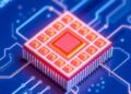
In the era of ever-increasing digital communication, the backbone of modern data transmission relies heavily on the swift, seamless flow of information carried by pulses of light through fiber-optic networks. Each second, billions of emails, viral TikTok videos, and complex artificial intelligence (AI) computations traverse global networks, riding on these optical pulses. At the heart of this vast data movement are photonic chips, tiny yet powerful components that not just carry but also manipulate light signals. These chips perform critical tasks, directing and integrating light within intricate networks. However, current photonic technologies face intrinsic limitations, especially when performing essential operations like signal conversion and amplification, which still depend on supplementary components that introduce bottlenecks in terms of size, power consumption, and heat dissipation.
The fast-evolving landscape of generative AI intensifies these challenges. Unlike traditional data queries, AI workloads involve continuous, interactive exchanges between processors. This increased communication necessitates frequent transformations and reshaping of optical signals, magnifying the energy consumption associated with these conversions. What used to be a trivial fraction of the total power usage in data centers is now becoming a formidable energy hurdle. With digital infrastructure already accounting for approximately 2% of global electricity consumption, the rising computational demands risk triggering rapid energy escalations, potentially compromising the scalability and sustainability of AI systems.
Amidst these mounting challenges, a research group led by Professor Stéphane Kéna-Cohen at Polytechnique Montréal has made a groundbreaking discovery that could pave the way for a new paradigm in integrated photonics. Their findings, recently published in the acclaimed journal Science Advances, unveil an innovative approach to integrate advanced light-processing capabilities directly onto silicon photonic chips. This method bypasses the traditional need for energy-intensive conversions between electrical and photonic signals, allowing light to be processed natively on chip, thereby enhancing efficiency and performance.
Central to this breakthrough is the identification of a novel organic molecule, triphenylamine–dicyanoquinoxaline, or TPA-QCN, which possesses exceptional second-order optical nonlinearity. This property enables light beams to interact within the material matrix, a requisite for advanced optical operations such as amplification and modulation. By harnessing TPA-QCN, researchers have opened the door to various integrated photonic functions previously unattainable or limited by existing silicon-based technologies.
What makes TPA-QCN particularly compelling is its deposition methodology and molecular alignment. Through vacuum evaporation, the material is applied as a thin film on silicon substrates. Unlike disordered arrangements seen in many organic films, TPA-QCN molecules spontaneously adopt a preferred orientation within the film. This self-aligned configuration is crucial because it fundamentally modifies how the material interacts with light, endowing it with unique capabilities unattainable by conventionally structured films or silicon alone. According to Kéna-Cohen, this subtle molecular behavior is what confers the material’s ability to manipulate optical signals innovatively.
From a manufacturing perspective, the compatibility of this organic thin film with established industry fabrication processes heralds a practical and scalable path forward. The deposition occurs at low temperatures and low costs, making it conducive for integration into existing photonic chip production lines without substantial retooling. Pierre-Luc Thériault, the primary author of the study, emphasizes the feasibility of this approach, highlighting its potential to incorporate new optical functionalities directly onto photonic chips without compromising the production ecosystem.
To exemplify the practical application of their discovery, the researchers engineered an integrated photonic device capable of converting infrared light, commonly utilized in telecommunication networks, into visible red light within the chip. This demonstration serves as a proof of principle, showcasing the material’s capacity for on-chip wavelength conversion—a critical functionality for future optical communication and quantum information processing. Encouragingly, subsequent advances with enhanced molecular variants of TPA-QCN hint at even greater performance capabilities.
The implications of this work are profound for the future of photonics and AI hardware. The integration of functions such as modulation, amplification, and light source generation on a single chip can simplify architectures, reduce the number of optical-electrical conversion steps, and mitigate heat generation. Such improvements translate into energy efficiency gains and bolster the performance limits of data centers grappling with the escalating throughput demands imposed by AI.
Recent developments in AI-specific hardware, including Google’s TPU 8t and 8i chips, underscore how evolving computing architectures are intensifying the demands on data transmission infrastructure. The increasing frequency of data exchanges between processors renders optical signal movement a critical bottleneck. Innovations like Polytechnique Montréal’s organic photonic films could thus act as a vital enabler for sustaining AI’s rapid advancement, empowering photonics to shoulder a greater role in data processing rather than merely serving as a passive conduit for light.
Looking ahead, integrating these advanced optical materials heralds a new generation of photonic components that could revolutionize signal processing, quantum technology, and telecommunication. By merging multiple light manipulation capabilities on compact silicon platforms with improved energy profiles, these innovations promise to transform the scale and scope of digital infrastructure. As AI continues to reshape how information is generated and consumed, next-generation photonics will be key to keeping pace sustainably.
The scientific community eagerly anticipates further developments and refinements in this domain, where materials science, optics, and device engineering converge to overcome looming energy and performance barriers. This landmark study illuminates a future where light itself is not only the messenger but also the active processor of data, seamlessly embedded within the very chips that drive our digital world.
Subject of Research: Not applicable
Article Title: Poling-free integrated second-order nonlinear optics with evaporated organic thin films
News Publication Date: 27-May-2026
Web References:
Expert profile – Stéphane Kéna-Cohen
Department of Engineering Physics, Polytechnique Montréal
Science Advances Article DOI
References:
Science Advances, article DOI: 10.1126/sciadv.aeg3170
Image Credits: Caroline Perron
Keywords
Integrated photonics, organic thin films, second-order nonlinear optics, TPA-QCN, silicon photonic chips, AI hardware scalability, optical signal conversion, energy-efficient data centers, infrared to visible light conversion, photonic amplification, molecular self-alignment, quantum technology photonics
Tags: challenges in photonic signal conversionenergy-efficient photonic technologiesfiber-optic networks for artificial intelligencegenerative AI data communicationheat dissipation in photonic devicesintegrated photonic chips for AIoptical signal amplification bottlenecksphotonic chips in data transmissionpower consumption in AI data centersreducing energy use in AI workloadsscaling AI with optical communicationsustainable digital infrastructure for AI