For decades, the field of semiconductor research has yielded relatively incremental advancements, especially considering the maturity of the materials involved. However, a recent breakthrough by researchers at Stanford University promises to redefine the operational landscape of infrared (IR) light-emitting diodes (LEDs) and sensors. Utilizing a century-old class of semiconductors known as IV-VI materials — specifically lead selenide (PbSe) and lead tin selenide (PbSnSe) — the team has demonstrated innovative integration methods with contemporary semiconductor technology. This development sets the stage for advances in compact, affordable, and efficient infrared devices poised to impact environmental monitoring, medical diagnostics, and industrial sensing.
At the core of this research is the realization that these IV-VI semiconductor thin films, despite their long scientific history, offer unique optoelectronic properties when manipulated at the nanoscale. Senior author Kunal Mukherjee, assistant professor of materials science and engineering at Stanford’s School of Engineering, emphasizes the significance: “We taught an old dog new tricks.” Unlike traditional semiconductors, these materials are tailored to emit in the mid-infrared wavelength range (4000-5000 nm), ideally suited for detecting greenhouse gases in the atmosphere or for use in medical carbon dioxide sensing technologies. These specific wavelengths represent a critical spectral “window” for monitoring environmental and physiological phenomena.
A remarkable aspect of these IV-VI based devices lies in their defect tolerance. Nanocrystalline semiconductors conventionally require atomic-level precision in their fabrication to suppress defects that could otherwise hamper electronic performance or optical output. The Stanford team’s diodes, however, exhibited robust operation despite harboring billions of dislocations and other crystal imperfections per square centimeter. This tolerance to structural defects significantly relaxes stringent manufacturing constraints, ultimately lowering production costs and facilitating scalability within existing semiconductor fabrication infrastructures. The potential to leverage current manufacturing technology without extensive retooling marks an important industrial advantage.
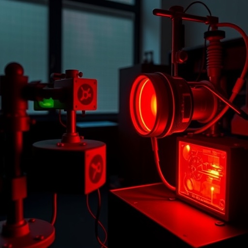
This breakthrough was not achieved overnight. Over a five-year investigative journey, the Stanford researchers meticulously employed molecular beam epitaxy (MBE), a highly controlled method of depositing atomic layers to craft complex semiconductor heterostructures. The painstaking nature of this atom-by-atom growth process underscored the project’s complexity and the degree of precision required, even if the endpoint devices can tolerate defects. Graduate student Jarod Meyer, a key contributor, recounts the relentless dedication needed to maintain MBE equipment and environmental stability to ensure the crystal quality essential for device performance.
Their first publication, appearing in Advanced Optical Materials, details the successful integration of IV-VI materials with more conventional III-V semiconductors like gallium arsenide (GaAs). This hybrid lattice-mismatched heterojunction formation allowed the team to fabricate the unique mid-infrared LEDs. Though such lattice mismatches historically pose challenges in epitaxial growth leading to strain and defects, the group’s approach produced an efficient infrared platform that leverages both materials’ strengths. The luminosity of these LEDs exceeded expectations, despite operating within the defect-laden environments.
In parallel, a second complementary study published in Nano Letters introduces a novel technique to manipulate the crystal structure of PbSnSe films through precise temperature control. By toggling between two ordered crystalline phases separated by a distinct phase boundary, they demonstrated dynamic modulation of infrared light transmission. This phase change is not between ordered and disordered states, as is typical in other phase-change materials, but between two well-defined ordered states, maintaining crystalline coherence with the underlying GaAs substrate. This finding advances the ability to fine-tune optical properties such as intensity, phase, and polarization of transmitted infrared light, broadening potential device functionality.
The practical effect of these phase transitions in the material is profound: the IR light can be actively switched between transparent and opaque states within sub-micrometer thin films. As a result, the engineered devices can function as modulators or optical switches in mid-infrared systems, essential components in communication, sensing, and imaging technologies. Controlling IR light at such a granular level opens avenues for integrating these materials in photonic circuits and adaptive optics platforms.
Historically, the LED industry’s focus has been primarily on visible light emission, yielding mature technologies for consumer electronics and lighting. Infrared LEDs and related sensors, conversely, have faced lagging development characterized by bulky, costly, and inefficient designs. Stanford’s innovation challenges this paradigm by proposing sleek, cost-effective IR devices compatible with existing semiconductor production lines. Mukherjee envisions a new generation of IR components—affordable, scalable, and seamlessly integrable—that can permeate applications from environmental gas detection to industrial process control and non-invasive health monitoring.
This revamped approach to IR photonics also leverages well-understood IV-VI materials, merging their inherent mid-infrared responsiveness with reliable III-V semiconductor platforms. The ability to mechanically and thermally induce reversible phase changes in these materials affords engineers newfound control over device performance, surpassing static designs. Such dynamic device architectures could redefine infrared sensing capabilities with faster response times, enhanced sensitivity, and lower power consumption.
Moreover, the flexible fabrication process championed by the Stanford team presents compelling economic incentives. The defect tolerance of these devices alleviates the need for ultra-pure crystal growth, significantly cutting costs and simplifying scalability. Operational devices with billions of atomic-level defects could be produced more rapidly and affordably, accelerating the translation from laboratory prototypes to commercial offerings. This compatibility with existing chip fabrication infrastructure ensures that these mid-infrared LEDs and sensors can be manufactured en masse without prohibitive capital expenditures.
Looking forward, Mukherjee and his colleagues anticipate multiple technological frontier expansions. The devices could enable widespread deployment of environmental monitoring tools able to detect trace gases and pollutants with greater accuracy. In medicine, advanced sensors could power breath analyzers or metabolic monitors with enhanced IR detection capability. Industrial applications may include precision non-contact temperature measurements and process control systems that leverage finely tunable infrared transmission.
Ultimately, this breakthrough illuminates a promising avenue for overcoming prior barriers in mid-infrared photonics. By resurrecting and modernizing century-old semiconductors through sophisticated epitaxial engineering and structural manipulation, Stanford’s materials engineers have opened the door to a transformative era of infrared devices. The synergy of novel materials science with established semiconductor technology forecasts a new dawn where infrared LEDs and sensors become ubiquitous, affordable, and highly functional, unlocking unprecedented capabilities across multiple sectors.
Subject of Research: Mid-infrared light-emitting diodes and phase-change semiconductor heterojunctions based on lead selenide and lead tin selenide integrated with gallium arsenide.
Article Title: Mid-Infrared LEDs Based on Lattice-Mismatched Hybrid IV–VI/III–V Heterojunctions
News Publication Date: 16-Feb-2026
Web References:
http://dx.doi.org/10.1002/adom.202503448
https://pubs.acs.org/doi/full/10.1021/acs.nanolett.5c04974
Image Credits: Stanford Engineering | Pooja Reddy
Keywords
Light emitting diodes, Diodes, Electronics, Electrical engineering, Infrared radiation, Semiconductors
Tags: affordable compact infrared devicesenvironmental monitoring infrared sensorsindustrial infrared sensing devicesinfrared light-emitting diodes advancementsIV-VI semiconductor materialslead selenide infrared technologylead tin selenide sensorsmedical diagnostics carbon dioxide sensingmid-infrared wavelength emissionnanoscale semiconductor integrationsemiconductor thin film innovationStanford University semiconductor research


