In a remarkable advance poised to reshape the landscape of photonics and silicon-based optoelectronics, a collaboration of researchers led by Professor Dries Van Thourhout at Ghent University – imec, Belgium, has unveiled an innovative class of nano-ridge surface-emitting lasers (NRSELs) directly epitaxially grown on standard 300 mm silicon wafers. This breakthrough, documented in the prestigious journal Light: Science and Applications, bypasses longstanding obstacles in vertical cavity surface-emitting laser (VCSEL) technology by harnessing one-dimensional photonic crystal modes and symmetry-protected bound states in the continuum. These elements combine to enable scalable, tunable surface emission from compact, wafer-integrated devices with broad applications ranging from telecommunications to sensing.
Traditional VCSELs have been a linchpin in data communication and consumer electronics such as optical mice and biometric authentication in smartphones. Nonetheless, their intricate construction—a multi-layer epitaxial stack comprising top and bottom distributed Bragg reflectors (DBRs) enveloping an active region—introduces severe fabrication complexities. The necessity for numerous precisely engineered mirror layers not only elongates growth time but also restricts wavelength agility, confining practical devices to emission around 850 nm and 980 nm. This limitation significantly hinders efforts to diversify emission bands or create multi-wavelength arrays on a single silicon platform, complicating the quest for seamless monolithic integration with silicon photonics and electronics.
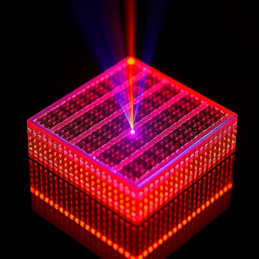
The pioneering NRSEL approach shatters these barriers by adopting aspect ratio trapping and nanostructure engineering techniques to cultivate high-quality III-V semiconductor materials directly on silicon substrates. This material forms ordered, one-dimensional nano-ridge arrays that themselves act as photonic crystals. Crucially, this architecture supports a symmetry-protected bound state in the continuum (BIC) mode, which simultaneously facilitates strong lateral confinement within the array and vertical emission out of the plane. The consequence is a compact surface-emitting laser whose cavity size and emission wavelength are governed by the nano-ridge geometry and periodicity—parameters amenable to precise design and wafer-scale scalability.
Unlike the vertically stacked mirrors of conventional VCSELs, the NRSEL’s reflectivity and lasing conditions are dictated by photonic crystal phenomena arising in the lateral dimension. This distinction offers unprecedented tuning versatility: emission wavelengths can be tailored across the wafer by adjusting the nano-ridge width and the interval between ridges. Further, dielectric overlays can fine-tune wavelengths post-growth, thereby granting an adaptability that was previously unattainable. Professor Van Thourhout highlights that while VCSELs are constrained by stringent wavelength and growth complexities, the NRSEL design paradigm elevates the emission wavelength to a flexible design variable, making complex, multi-wavelength on-chip laser arrays a tangible reality.
Fundamentally, the physics exploited here harks back to a nearly century-old quantum mechanical concept. The BIC, first theorized by von Neumann and Wigner in 1929, represents a counterintuitive mode that remains confined within the continuum of radiation states due to symmetry protection. In the NRSEL system, this means the laser mode is tightly confined in-plane within the nano-ridge cavity yet retains the capacity for efficient vertical light extraction. This elegant mode confinement mechanism permits surface-emitting lasers with a diminutive footprint—nano-ridges of merely 500 nanometers in height—epitaxially grown atop silicon, sidestepping the cumbersome vertical mirror stacks and facilitating integration with silicon photonic circuits.
The NRSEL does not merely serve as a gain medium. The nano-ridges themselves simultaneously perform multiple critical functions: they define the active region, form the resonant cavity, confine the optical mode, and act as the out-coupling structure for surface emission. This multifunctionality significantly reduces device complexity and footprint while enhancing performance and manufacturability. The seamless mode confinement and emission characteristics within nanoscale dimensions open new horizons for high-density laser integration on silicon wafers used in mass production.
Moreover, the technology leverages the manufacturing assets of the semiconductor industry by using standard 300 mm silicon wafers as the growth substrate, enabling compatibility with established wafer-scale processing and co-integration with other photonic and electronic elements. This represents a pivotal step toward creating fully integrated silicon photonic chips with embedded laser sources, a target long sought after in the fields of optical interconnects and on-chip sensing. While the current demonstration employs optical pumping, the team envisions leveraging their previous successes with electrically injected in-plane nano-ridge lasers to realize electrically pumped NRSELs, contingent on engineering contacts that preserve optical mode integrity and permit unobstructed vertical emission.
Eslam Fahmy, the study’s first author and a doctoral candidate, emphasizes the novelty and significance of this platform, noting that it combines compactness, wavelength tunability, and compatibility with large-scale manufacturing in a manner rarely achieved with traditional surface-emitting lasers. The NRSEL’s ability to merge photonic crystal physics with practical device engineering on silicon heralds new horizons for integrated photonics, promising advancements in diverse application spaces, including high-speed optical communication, LIDAR, bio-sensing, and quantum information processing.
This groundbreaking work is emblematic of a broader movement toward integrating multifunctional optical components directly within silicon photonics ecosystems, which until now have been hindered by the poor compatibility of direct laser sources. By eliminating complex DBR mirrors and replacing them with engineered nano-ridge arrays exhibiting symmetry-protected bound states, these lasers achieve performance metrics previously locked behind material and fabrication hurdles. The architecture opens pathways to customizable wavelength arrays on a single chip, further bolstering the roadmap for photonic integration.
In synthesis, the NRSEL represents a revolutionary advance, elegantly solving long-standing problems in the field by turning wavelength specificity into a design degree of freedom and by harnessing quantum-mechanical mode confinement concepts within scalable epitaxial growth processes. As research progresses toward electrically driven devices and hybrid photonic-electronic circuits, the impact of this technology is expected to ripple across disciplines, from telecommunications infrastructure to consumer electronics and emerging quantum technologies.
This achievement foregrounds the importance of cross-disciplinary expertise in quantum optics, photonic engineering, and semiconductor materials science, proving that the fusion of classical and quantum concepts can deliver tangible breakthroughs in device fabrication. The team’s approach validates the strategic vision of co-integrating active optical sources directly on silicon, contributing decisively to the long-standing objective of creating fully integrated photonic chips with embedded, wavelength-tunable laser arrays fabricated on industrial-scale silicon wafers.
As Professor Van Thourhout and his colleagues continue to refine the electrical injection mechanisms and optimize wavelength control, the prospect of deploying compact, scalable laser sources for silicon photonics appears closer than ever. This milestone stands as a testament to how fundamental physics, when combined with cutting-edge materials engineering, can catalyze transformative technological innovation directly impacting the future of optical communication and sensing platforms.
Subject of Research: Nano-ridge surface emitting lasers epitaxially grown on standard 300 mm silicon wafers utilizing one-dimensional photonic crystal modes and bound states in the continuum.
Article Title: One-dimensional photonic crystal nano-ridge surface emitting lasers epitaxially grown on a standard 300 mm silicon wafer
Web References:
https://doi.org/10.1038/s41377-025-02061-z
Image Credits: Dries Van Thourhout et al.
Keywords
Nano-ridge lasers, surface-emitting laser, silicon photonics, photonic crystals, bound states in the continuum, epitaxial growth, wavelength tunability, silicon integration, III-V semiconductors, vertical cavity surface-emitting laser, quantum optics, optical communication
Tags: epitaxial growth on silicon wafersmonolithic integration of lasers on siliconmulti-wavelength laser arrays on siliconnano-ridge surface-emitting lasersone-dimensional photonic crystal lasersphotonic crystal modes in lasersscalable wafer-integrated laserssilicon-based optoelectronics advancementssymmetry-protected bound states in the continuumtelecom and sensing laser applicationstunable surface emission devicesVCSEL technology limitations


