Quantum physics continues to astonish researchers by unveiling phenomena that challenge classical intuition and reveal hidden patterns in the seemingly random fabric of the microscopic world. A groundbreaking new theoretical study has advanced our understanding of quantum scarring—an enigmatic quantum phenomenon that bridges quantum dynamics and classical mechanics—and showcased its profound implications for electron transport in nanoscale devices. This latest research not only clarifies how quantum scars influence electron flow but also paves the way for innovative nanotechnologies and the emergent field of “scartronics,” signaling a paradigm shift in how we conceptualize conductivity in quantum-scale structures.
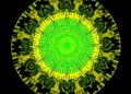
At its core, quantum mechanics describes the behavior of particles such as electrons and photons at atomic and subatomic scales, where the rules of classical physics give way to probabilistic wave functions and uncertainty. Typically, in chaotic quantum systems where components interact strongly and unpredictably, electron wavefunctions tend to spread diffusely, reflecting an absence of regular dynamics. Yet, paradoxically, quantum scars are localized regions where electron probability densities concentrate along paths reminiscent of unstable classical trajectories. First discovered in the 1980s, these scars defy expectations by revealing latent order within chaos, creating fingerprint-like patterns that imprint dynamical memory onto quantum states.
Building on previous pioneering work from researchers at Tampere University and Harvard University, who first demonstrated the formation of distinctive quantum scar patterns known as “quantum Lissajous scars” within nanostructures, the current study delves deeper into the functional ramifications of these scars. It reveals how quantum scars can dramatically enhance electronic conduction within open quantum dots—nanostructures that confine electrons in two dimensions but are coupled to external electrodes enabling electric current. By linking theory with experiment, the team illuminates the practical potential of scarring to act as a nanoscale conduit for electron flow, akin to a switchable quantum channel.
One of the most remarkable insights from this work, led by doctoral researcher Fartash Chalangari, is the transformation of imperfections—typically detrimental in nanoscale devices—into advantageous features that bolster electron transport. These scarred states consolidate pathways that promote coherent electron propagation rather than scattering or decoherence. This discovery fundamentally challenges conventional wisdom that defects always impede performance, suggesting instead that precise control over quantum scars could be harnessed to optimize device characteristics and energy efficiency.
The research rigorously explores variational methods to characterize scarring phenomena within open two-dimensional quantum dots. By employing sophisticated computational models and numerical simulations, the team quantifies how the morphology and strength of quantum scars depend on device geometry, potential landscape, and electrode coupling. Their findings indicate that quantum scars serve as robust quantum channels that sustain high electron transmission, despite environmental perturbations and inherent system disorder. This resilience positions quantum scars as promising building blocks for next-generation nanoelectronic components.
From a technological perspective, enhanced electron flow mediated by quantum scars provides a pathway to realize novel nanoscale transistors and switches that operate with minimal power consumption and maximal speed. Unlike classical transistors relying on gate voltages to modulate current, scar-based devices exploit intrinsic quantum interference effects that arise naturally within the material’s architecture. Such components could hence revolutionize microchip design, enabling ultra-compact integrated circuits with performance vastly outperforming current silicon-based technology.
Moreover, quantum scarring opens exciting avenues in the domain of quantum information processing. Although practical quantum computers remain a longer-term goal, the highly coherent and controllable electron states represented by scars may serve as prototype qubits or quantum channels, providing new routes for coherent control and error mitigation. The ability to deliberately engineer and manipulate scar states using charged nanoprobes or geometrical tuning could thus contribute to scalable quantum computing hardware architectures.
The interdisciplinary collaboration between Tampere University’s Quantum Control and Dynamics research group and Harvard University exemplifies the merging of theoretical physics with experimental nanoscience. Their combined efforts have already yielded experimental observations of scar-enhanced conductivity in graphene-based systems, demonstrating the generalizability and physical reality of scartronics beyond idealized quantum dots. These cross-institutional advances underscore a future where quantum effects can be tailored and exploited rather than merely observed.
Experimental techniques such as scanning tunneling microscopy with charged nanotips have been instrumental in visualizing and controlling quantum scars in situ. These tools allow researchers to selectively modify local electrostatic potentials, effectively tuning scar patterns and investigating their influence on conduction pathways. This level of control ushers in a new era of nanoscale device engineering driven by quantum wavefunction design, elevating quantum scarring from a curious phenomenon to a functional mechanism.
While the practical applications of quantum scars in commercial technologies may still lie ahead, this research marks a milestone in fundamental quantum science. It reveals how emergent order arises within chaotic systems and provides a blueprint for transforming such phenomena into technological innovations. By shifting the paradigm from avoiding imperfections to leveraging them as resources, the field of scartronics promises to impact microelectronics, quantum computing, and materials science profoundly.
In summary, the research article “Variational Scarring in Open Two-Dimensional Quantum Dots,” published in Physical Review B on 17 September 2025, heralds a new chapter in quantum physics. It bridges theoretical insight, computational modeling, and experimental validation to elucidate the role of quantum scars in enhancing electron transport and device performance. This breakthrough not only enriches our understanding of the quantum-classical interface but also lays the groundwork for the next generation of nanoscale quantum devices driven by the elegant interplay of chaos and order.
The quantum control achieved over these scars, as described by Professor Esa Räsänen and colleagues, may eventually unlock avenues for creating energy-efficient electronic components and novel qubit designs, catalyzing progress across both classical and quantum technologies. Supported by robust funding from the Research Council of Finland, CSC – IT Center for Science, and the U.S. National Science Foundation, this research exemplifies cutting-edge exploration into the frontier of quantum nanoscience.
Subject of Research: Quantum scar phenomena and their impact on electron transport in nanoscale open quantum dots.
Article Title: Variational Scarring in Open Two-Dimensional Quantum Dots
News Publication Date: 17 September 2025
Web References:
Article DOI: 10.1103/37qq-bd15
Related article on quantum Lissajous scars: https://doi.org/10.1103/PhysRevLett.123.214101
Image Credits: Quantum Control and Dynamics research group, Tampere University
Keywords
Quantum scars, quantum chaos, electron transport, nanoscale devices, quantum dots, scartronics, nanotechnology, quantum interference, variational methods, graphene, quantum computing, microchips
Tags: advanced microchip developmentchaotic quantum systems and electron behaviorconductivity in quantum-scale structureselectron transport in nanoscale devicesimplications of quantum dynamicsinnovative nanotechnologieslocalized electron probability densitiesquantum mechanics and classical physicsquantum scarring phenomenonresearch in quantum physicsscartronics in nanotechnologyunderstanding quantum chaos
