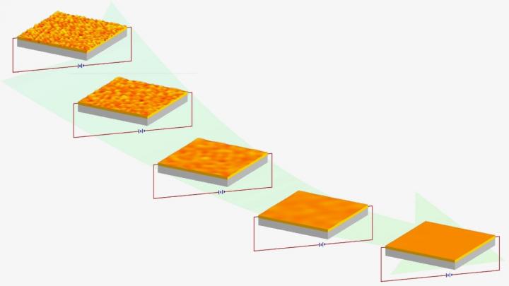
Credit: Du and Maroudas
WASHINGTON, D.C., March 7, 2017 — Surface roughness reduction is a really big deal when it comes to fundamental surface physics and while fabricating electronic and optical devices. As transistor dimensions within integrated circuits continue to shrink, smooth metallic lines are required to interconnect these devices. If the surfaces of these tiny metal lines aren't smooth enough, it substantially reduces their ability to conduct electrical and thermal energy — decreasing functionality.
A group of engineers at the University of Massachusetts Amherst are now reporting an advance this week in Applied Physics Letters, from AIP Publishing, in the form of modeling results that establish electrical surface treatment of conducting thin films as a physical processing method for reducing surface roughness.
"We've been thinking hard about this roughness problem for many years, since showing that electric currents can be used to inhibit surface cracking," said Dimitrios Maroudas, co-author and a professor in the Department of Chemical Engineering. "So as soon as we developed the computational tools to attack the full film roughness problem, we got to work."
The group's work focused on using a copper film on a silicon nitride layer to quantify the model parameters for their simulations and make comparisons with available experimental findings, which they were able to reproduce.
"Surface electromigration is the key physical concept involved," Maroudas explained. "It's the directed transport of atoms on the metal surface due to the so-called electron wind force, which expresses the transfer of momentum from the electrons of the metal moving under the action of an electric field to the atoms (ions) — biasing atomic migration."
Think of it as akin to the diffusion of ink in flowing water. "Electromigration's role in the transport of surface atoms is analogous to that of convection due to flow on the transport of ink within the water," Maroudas said. "The combined effects of a well-controlled applied electric field and rough surface geometry drive the atoms on the metal surface to move from the hills of the rough surface morphology to the neighboring valleys, which eventually smooth away the rough surfaces."
This work is significant, particularly within the microelectronics realm, because it establishes the electrical treatment of metallic (conducting) films as a viable physical processing strategy for reducing their surface roughness.
"Our approach is qualitatively different than traditional mechanical polishing or ion-beam irradiation techniques," said Lin Du, co-author and a doctoral student working with Maroudas. "It directly influences the driven diffusion of surface atoms precisely, which affects surface atomic motion and enables a smooth surface all the way down to the atomic level."
The required electric field action can be conveniently controlled macroscopically: simply choose a direction, adjust the voltage, and flip a switch "on."
"While studying the phenomenon, we discovered that a sufficiently strong electric field can bring the metallic surface to an atomically smooth state," Du said. "The required electric field strength depends largely on the field direction and surface material properties of the metallic film — such as film texture and surface diffusional anisotropy, because in surfaces of crystalline materials diffusion is faster along certain preferred directions."
A true irony here is that "electromigration is best known for its damaging effects within metallic interconnects — underlying crucial materials reliability problems in many generations of microelectronics," Maroudas said.
As far as applications, since this work establishes the principles to create smoother conducting material surfaces, "it can be used for fabricating and processing nanoscale-thick metallic components within electronic and optical devices, which require atomic-scale smoothness," Maroudas said. "The ability to reduce the surface roughness of metallic components, such as interconnects within integrated circuits, will significantly improve their performance as well as durability and reliability."
What's the next step for the engineers? "We're currently exploring how the effectiveness of the method depends on the metallic film texture (or surface crystallographic orientation), the film's wetting of the substrate, and the electric field direction with respect to certain surface crystallographic directions," Maroudas said.
The group's immediate goal is "to optimize the electrical treatment technique, and to identify the conditions for minimizing the required electric field strength, as well as the cost of applying this technique," he added. "Our next natural step should be a partnership with an experimental laboratory with the proper expertise to carry out tests that will help us move from proof of concept to an enabling technology."
###
The article, "Current-induced surface roughness reduction in conducting thin films," is authored by Lin Du and Dimitrios Maroudas. The article will appear in the journal Applied Physics Letters March 7, 2017 (DOI: 10.1063/1.4977024). After that date, it can be accessed at http://aip.scitation.org/doi/full/10.1063/1.4977024.
ABOUT THE JOURNAL
Applied Physics Letters features concise, rapid reports on significant new findings in applied physics. The journal covers new experimental and theoretical research on applications of physics phenomena related to all branches of science, engineering, and modern technology. See http://apl.aip.org.
Media Contact
Julia Majors
[email protected]
301-209-3090
@jasonbardi
http://www.aip.org
############
Story Source: Materials provided by Scienmag


