
In a groundbreaking advancement in terahertz wave generation, researchers at the Massachusetts Institute of Technology (MIT) have introduced an innovative approach that promises to revolutionize the use of these high-frequency waves in various applications. Terahertz waves—occupying a unique position on the electromagnetic spectrum between radio waves and infrared light—have significant potential due to their ability to facilitate faster data transmission, enhance medical imaging precision, and improve radar resolution. However, the practical generation of these waves using compact semiconductor chips has long been a challenge.
Traditionally, generating terahertz waves with sufficient radiating power for practical applications has necessitated the use of bulky, expensive silicon lenses. These lenses are often larger than the chips themselves, resulting in integration difficulties within electronic devices. The research team at MIT sought to address this critical bottleneck by developing a terahertz amplifier-multiplier system that can achieve higher radiating power while eliminating the need for silicon lenses altogether. This innovative system is a compelling leap forward in the quest for compact, efficient, and scalable terahertz wave generators.
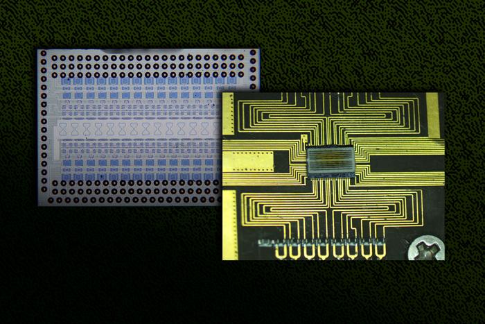
The researchers were able to enhance the efficiency of their chip-based terahertz wave generator by affixing a thin, patterned sheet of material to the back of the chip. This key innovation hinged on the use of higher-power Intel transistors, which significantly increased the chip’s performance. Importantly, this new chip-based solution maintains a compact profile, making it suitable for a variety of applications, such as advanced security scanners and environmental monitoring devices.
Jinchen Wang, a graduate student in electrical engineering at MIT and the lead author of the research, emphasized the importance of scalability in their design. The advancement allows for the creation of terahertz arrays composed of hundreds of chips, which cannot accommodate traditional silicon lenses due to space constraints. The researchers demonstrated a promising approach that effectively combines performance with low manufacturing costs, paving the way for the development of practical terahertz devices.
To generate these terahertz waves, researchers utilized a CMOS chip-based amplifier-multiplier chain. This system escalates the frequency of radio waves into the terahertz range. Traditionally, the emitted waves pass through the silicon chip and are released into the open air. However, an inherent property of materials known as the dielectric constant poses challenges to the efficiency of this process. The researchers observed that the dielectric constant of silicon is substantially higher than that of air, leading to significant signal reflection at the silicon-air interface which impairs overall efficiency.
In contrast to current methods that rely on supplementary silicon lenses to enhance signal strength, the MIT researchers took an innovative route by applying the concept of electromagnetic matching. By matching the dielectric constants of silicon and air, they aimed to minimize signal reflection at this critical boundary. This was achieved by affixing a thin sheet material to the back of the chip, which possesses a dielectric constant that falls between silicon and air, allowing more terahertz waves to be transmitted outward.
To attain optimal performance from the matching sheet, the researchers selected a commercially available substrate material with properties closely aligned to their requirements. They further refined this material using laser cutting techniques to create subwavelength holes. These modifications lowered the dielectric constant of the sheet and significantly improved signal transmission efficiency. This combination of strategic material selection and advanced fabrication techniques resulted in a notable enhancement of the chip’s capabilities.
Additionally, the implementation of specialized transistors developed by Intel—known for their superior maximum frequency and breakdown voltage characteristics—played a crucial role in elevating the performance of the terahertz wave generation system. The collaborative efforts of these components enabled the MIT researchers to surpass the performance metrics of various existing terahertz devices on the market.
The newly developed chip was capable of generating terahertz signals with a peak radiation power of 11.1 decibel-milliwatts, a leading figure amongst current state-of-the-art technologies. Moreover, the affordability of the chip allows for scalable production, facilitating seamless integration into real-world electronic systems. Researchers highlighted that one of the major challenges in scalable chip development involved effectively managing power and temperature while generating terahertz waves.
Given the high frequencies and power levels involved, many conventional CMOS chip design methodologies were not applicable. Addressing this issue demanded innovative thinking and tailored solutions. Additionally, the research team is preparing to launch a practical demonstration of their technology, which will involve the fabrication of a phased array of terahertz sources that will be able to steer and focus powerful terahertz beams through compact, cost-effective devices.
In conclusion, MIT’s groundbreaking advances in terahertz wave generation reflect the potential of modern technology to overcome longstanding challenges in semiconductor applications. By developing a scalable, efficient chip-based solution that circumvents the need for unwieldy silicon lenses, the researchers are laying the groundwork for enhanced applications in various fields, including telecommunications, medical diagnostics, and environmental science. Their innovative approach not only represents a significant step forward in terahertz technology but also illuminates exciting possibilities for future research and practical implementation.
Subject of Research: Terahertz Wave Generation
Article Title: MIT Researchers Revolutionize Terahertz Wave Generation with Innovative Chip-Based Design
News Publication Date: October 2023
Web References: [N/A]
References: [N/A]
Image Credits: MIT News
Keywords
Terahertz waves, semiconductor technology, data transmission, medical imaging, radar resolution, chip-based systems, scalable design, JSON chip technology, electromagnetic matching, silicon lenses, amplifier-multiplier systems.
Tags: challenges in terahertz wave practical applicationscompact terahertz wave generatorsefficient data transmission terahertz technologyeliminating silicon lenses in electronicsenhanced medical imaging with terahertz waveshigh-frequency electromagnetic spectrum applicationsinnovative materials for terahertz efficiencyMIT terahertz amplifier-multiplier systemradar resolution improvement using terahertzscalable terahertz wave systemssemiconductor chips for terahertz wavesterahertz wave generation technology


