A novel method that employs palladium to inject hydrogen into the deeply buried oxide-metal electrode contacts of amorphous oxide semiconductors (AOSs) storage devices, which reduces contact resistance, has been developed by scientists at Tokyo Tech. This innovative method presents a valuable solution for addressing the contact issues of AOSs, paving the way for their application in next-generation storage devices and displays.
Credit: Assistant Professor Masatake Tsuji and Honorary Professor Hideo Hosono
A novel method that employs palladium to inject hydrogen into the deeply buried oxide-metal electrode contacts of amorphous oxide semiconductors (AOSs) storage devices, which reduces contact resistance, has been developed by scientists at Tokyo Tech. This innovative method presents a valuable solution for addressing the contact issues of AOSs, paving the way for their application in next-generation storage devices and displays.
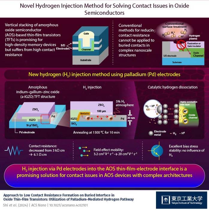
Thin film transistors (TFTs) based on amorphous oxide semiconductors (AOSs) have garnered considerable attention for applications in next-generation storage devices such as capacitor-less dynamic-random access memory (DRAM) and high-density DRAM technologies. Such storage devices employ complex architectures with TFTs stacked vertically to achieve high storage densities. Despite their potential, AOS TFTs suffer from contact issues between AOSs and electrodes resulting in excessively high contact resistance, thereby degrading charge carrier mobility, and increasing power consumption. Moreover, vertically stacked architectures further exacerbate these issues.
Many methods have been proposed to address these issues, including the deposition of a highly conductive oxide interlayer between the contacts, forming oxygen vacancies on the AOS contact surface and surface treatment with plasma. Hydrogen plays a key role in these methods, as it, when dissociated into atomic hydrogen and injected into the AOS-electrode contact area, generates charge carriers, thereby reducing contact resistance. However, these methods are energy-intensive or require multiple steps and while they effectively address the high-contact resistance of the exposed upper surface of the semiconductors, they are impractical for buried contacts within the complex nanoscale architectures of storage devices.
To address this issue, a team of researchers (Assistant Professor Masatake Tsuji, doctoral student Yuhao Shi, and Honorary Professor Hideo Hosono) from the MDX Research Center for Element Strategy at the International Research Frontiers Initiative at Tokyo Institute of Technology has now developed a novel hydrogen injection method. Their findings were published online in the journal ACS Nano on 22 March 2024.
In this innovative method, an electrode made up of a suitable metal, which can catalyze the dissociation of hydrogen at low temperatures, is used to transport the atomic hydrogen to the AOS-electrode interface, resulting in a highly conductive oxide layer. Choosing suitable electrode material is therefore key for implementing this strategy. Dr. Tsuji explains, “This method requires a metal that has a high hydrogen diffusion rate and hydrogen solubility to shorten post-treatment times and reduce processing temperatures. In this study, we utilized palladium (Pd) as it fulfils the dual role of catalyzing hydrogen dissociation and transport, making it the most suitable material for hydrogen injection in AOS TFTs at low temperatures, even at deep internal contacts.”
To demonstrate the effectiveness of this method, the team fabricated amorphous indium gallium oxide (a-IGZO) TFTs with Pd thin film electrodes as hydrogen transport pathways. The TFTs were heat-treated in a 5% hydrogen atmosphere at a temperature of 150 0C for 10 minutes. This resulted in the transport of atomic hydrogen by Pd to the a-IGZO-Pd interface, triggering a reaction between oxygen and hydrogen, forming a highly conductive interfacial layer.
Testing revealed that due to the conductive layer, the contact resistance of the TFTs was reduced by two orders of magnitude. Moreover, the charge carrier mobility increased from 3.2 cm2V–1s–1 to nearly 20 cm2V–1s–1, representing a substantial improvement. “Our method enables hydrogen to rapidly reach the oxide-Pd interface even in the device interior, up to a depth of 100 μm. This makes it highly suitable for addressing the contact issues of AOS-based storage devices” remarks Dr. Tsuji. Additionally, this method preserved the stability of the TFTs, suggesting no side effects due to hydrogen diffusion in the electrodes.
Emphasizing the potential of the study, Dr. Tsuji concludes: “This approach is specifically tailored for complex device architectures, representing a valuable solution for the application of AOS in next-generation memory devices and displays.” IGZO-TFT is now a de facto standard to drive the pixels of flat panel displays. The present technology will put forward its application to memory.
Journal
ACS Nano
DOI
10.1021/acsnano.4c02101
Method of Research
Experimental study
Subject of Research
Not applicable
Article Title
Approach to Low Contact Resistance Formation on Buried Interface in Oxide Thin-Film Transistors: Utilization of Palladium-Mediated Hydrogen Pathway
Article Publication Date
22-Mar-2024
COI Statement
The authors declare no competing financial interest.

