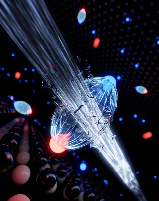
Semiconductors are ubiquitous in modern technology, working to either enable or prevent the flow of electricity. In order to understand the potential of two-dimensional semiconductors for future computer and photovoltaic technologies, researchers from the Universities of Göttingen, Marburg and Cambridge investigated the bond that builds between the electrons and holes contained in these materials. By using a special method to break up the bond between electrons and holes, they were able to gain a microscopic insight into charge transfer processes across a semiconductor interface. The results were published in Science Advances.
Credit: Lukas Kroll, Jan Philipp Bange, Marcel Reutzel, Stefan Mathias: Science Advances DOI: 10.1126/sciadv.adi1323
Semiconductors are ubiquitous in modern technology, working to either enable or prevent the flow of electricity. In order to understand the potential of two-dimensional semiconductors for future computer and photovoltaic technologies, researchers from the Universities of Göttingen, Marburg and Cambridge investigated the bond that builds between the electrons and holes contained in these materials. By using a special method to break up the bond between electrons and holes, they were able to gain a microscopic insight into charge transfer processes across a semiconductor interface. The results were published in Science Advances.
When light shines on a semiconductor, its energy is absorbed. As a result, negatively charged electrons and positively charged holes combine in the semiconductor to form pairs, known as excitons. In the most modern two-dimensional semiconductors, these excitons have an extraordinarily high binding energy. In their study, the researchers set themselves the challenge of investigating the hole of the exciton. As physicist and first author Jan Philipp Bange from the University of Göttingen explains: “In our laboratory, we use photoemission spectroscopy to investigate how the absorption of light in quantum materials leads to charge transfer processes. So far, we have concentrated on the electrons that are part of the electron-hole pair, which we can measure using an electron analyser. Up to now, we didn’t have any way to directly access the holes themselves. So, we were interested in the question of how we could characterise not just the electron of the exciton but also its hole.”
To answer this question, the researchers, led by Dr Marcel Reutzel and Professor Stefan Mathias at Göttingen University’s Faculty of Physics, used a special microscope for photoelectrons in combination with a high-intensity laser. In the process, the breaking up of an exciton leads to a loss of energy in the electron measured in the experiment. Reutzel explains: “This energy loss is characteristic for different excitons, depending on the environment in which the electron and the hole interact with each other.” In the current study, the researchers used a structure consisting of two different atomically thin semiconductors to show that the hole of the exciton transfers from one semiconductor layer to the other, similar to a solar cell. Professor Ermin Malic’s team at the University of Marburg was able to explain this charge transfer process with a model to describe what happens at a microscopic level.
Mathias summarises: “In the future, we want to use the spectroscopic signature of the interaction between electrons and holes to study novel phases in quantum materials at ultrashort time and length scales. Such studies can be the basis for the development of new technologies and we hope to contribute to this in the future.”
This research benefited from the German Research Foundation (DFG) funding for the Collaborative Research Centres “Atomic scale control of energy conversion” and “Mathematics of Experiment” in Göttingen and “Structure and Dynamics of Internal Interfaces” in Marburg.
Original publication: Bange et al., Probing electron-hole Coulomb correlations in the exciton landscape of a twisted semiconductor heterostructure, Science Advances (2024). DOI: 10.1126/sciadv.adi1323
Contact:
Professor Stefan Mathias
University of Göttingen
Faculty of Physics
Friedrich Hund Platz 1, 37077 Göttingen, Germany
Tel: +49 (0)551 39-27601
Email: [email protected]
www.mathiaslab.uni-goettingen.de
Dr Marcel Reutzel
University of Göttingen
Faculty of Physics
Friedrich Hund Platz 1, 37077 Göttingen, Germany
Email: [email protected]
Journal
Science Advances
DOI
10.1126/sciadv.adi1323
Method of Research
Experimental study
Subject of Research
Not applicable
Article Title
Probing electron-hole Coulomb correlations in the exciton landscape of a twisted semiconductor heterostructure
Article Publication Date
7-Feb-2024
