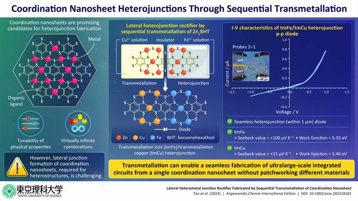
Electronically conducting two-dimensional (2D) materials are currently hot topics of research in both physics and chemistry owing to their unique properties that have the potential to open up new avenues in science and technology. Moreover, the combination of different 2D materials, called heterostructures, expands the diversity of their electrical, photochemical, and magnetic properties. This can lead to innovative electronic devices not achievable with a single material alone.

Credit: Hiroshi Nishihara from Tokyo University of Science
Electronically conducting two-dimensional (2D) materials are currently hot topics of research in both physics and chemistry owing to their unique properties that have the potential to open up new avenues in science and technology. Moreover, the combination of different 2D materials, called heterostructures, expands the diversity of their electrical, photochemical, and magnetic properties. This can lead to innovative electronic devices not achievable with a single material alone.
Heterostructures can be fabricated in two ways: vertically, with materials stacked on top of each other, or laterally, where materials are stacked side-by-side on the same plane. Lateral arrangements offer a special advantage, confining charge carriers to a single plane and paving the way for exceptional “in-plane” electronic devices. However, the construction of lateral junctions is challenging.
In this regard, conducting 2D materials made using organic materials, called “coordination nanosheets,” are promising. They can be created by combining metals and ligands, ranging from those with metallic properties such as graphene and semiconducting properties such as transition metal dichalcogenides to the ones possessing insulating properties such as boron nitride. These nanosheets enable a unique method called transmetallation. This allows the synthesis of lateral heterostructures with “heterojunctions,” which cannot be achieved through direct reaction. Heterojunctions are interfaces between two materials that have distinct electronic properties and therefore can serve as electronic devices. Furthermore, by utilizing heterojunctions of coordinated nanosheets, new electronic properties that have been difficult to get with conventional 2D materials can be created. Despite these advantages, the research on transmetallation as a method to fabricate heterostructures is still limited.
To address this knowledge gap, a team of researchers from Japan, led by Professor Hiroshi Nishihara from the Research Institute for Science and Technology at Tokyo University of Science (TUS), Japan, used sequential transmetallation to synthesize lateral heterojunctions of Zn3BHT coordination nanosheets. The team included Dr. Choon Meng Tan, Assistant Professor Naoya Fukui, Assistant Professor Kenji Takada, and Assistant Professor Hiroaki Maeda, also from TUS. The study, a joint research effort by TUS, the University of Cambridge, the National Institute for Materials Science (NIMS), Kyoto Institute of Technology, and the Japan Synchrotron Radiation Research Institute (JASRI), was published in the journal Angewandte Chemie International Edition on January 05, 2024.
The team first fabricated and characterized the Zn3BHT coordination nanosheet. Next, they investigated the transmetallation of Zn3BHT with copper and iron. Prof. Nishihara explains: “Via sequential and spatially limited immersion of the nanosheet into aqueous copper and iron ion solutions under mild conditions, we easily fabricated heterostructures with in-plane heterojunctions of transmetallated iron and copper nanosheets.”
This method is a solution process at room temperature and atmospheric pressure, from the fabrication of coordinated nanosheets to the fabrication of in-plane heterojunctions. This process is completely different from the high-temperature, vacuum, gas-phase processing process that is used in lithography technology for silicon semiconductors. It is a simple and inexpensive process that does not require large equipment. The challenge is how to create highly crystalline thin films that are free of impurities. If clean rooms and highly purified reagents are available, commercially viable manufacturing techniques will soon be achieved.
The resulting seamless heterojunction obtained by the researchers demonstrated rectifying behavior common in electronic circuits. Testing the characteristics of the diode revealed the versatility of the Zn3BHT coordination nanosheet. These characteristics can be changed easily without any special equipment. Moreover, this material also enables the fabrication of an integrated circuit from only a single coordination sheet, without any patchworking from different materials. Prof. Nishihara highlights the importance of this technique: “Ultrathin (nanometer-thick) rectifying elements obtained from our method will be quite useful for the fabrication of ultralarge-scale integrated circuits. Simultaneously, the unique physical properties of monoatomic layer films with in-plane heterojunctions can lead to the development of new elements.”
Furthermore, by using this transmetallation reaction, it is possible to create junctions with various electronic properties, such as p-n, MIM (metal-insulator-metal) and MIS (metal-insulator-semiconductor) junctions. The ability to bond single-layer topological insulators will also enable new electronic devices such as electron splitters and multilevel devices that have only been theoretically predicted.
Overall, this study presents a simple yet powerful technique for crafting lateral heterostructures, marking a significant step in 2D materials research.
***
Reference
DOI: https://doi.org/10.1002/anie.202318181
About The Tokyo University of Science
Tokyo University of Science (TUS) is a well-known and respected university, and the largest science-specialized private research university in Japan, with four campuses in central Tokyo and its suburbs and in Hokkaido. Established in 1881, the university has continually contributed to Japan’s development in science through inculcating the love for science in researchers, technicians, and educators.
With a mission of “Creating science and technology for the harmonious development of nature, human beings, and society,” TUS has undertaken a wide range of research from basic to applied science. TUS has embraced a multidisciplinary approach to research and undertaken intensive study in some of today’s most vital fields. TUS is a meritocracy where the best in science is recognized and nurtured. It is the only private university in Japan that has produced a Nobel Prize winner and the only private university in Asia to produce Nobel Prize winners within the natural sciences field.
Website: https://www.tus.ac.jp/en/mediarelations/
About Professor Hiroshi Nishihara from Tokyo University of Science
Dr. Hiroshi Nishihara is a Professor of Chemistry at Tokyo University of Science in Japan. He is a distinguished professor, researcher, and pioneer in the field of electrochemistry and the synthesis of conductive metal complex polymers. His research is focused on the creation of new electro- and photo-functional materials comprising both transition metals and π-conjugated chains, as well as the invention of unidirectional electron transfer systems using molecular layer interfaces. He has published more than 467 papers with over 14911 citations to his credit.
https://www.tus.ac.jp/ridai/doc/ji/RIJIA01Detail.php?act=&kin=ken&diu=6a2a&pri=en
https://www.rs.tus.ac.jp/nishihralab/index_en.html
Funding information
The study received financial support from JST-CREST JPMJCR15F2, JSPS KAKENHI Grant Number 19H05460, JSPS KAKENHI Grant Number 22K05055, JSPS KAKENHI Grant Number 22K14569, EPSRC-JSPS core-to-core Program (EP/S030662/1, JPJSCCA20190005), White Rock Foundation, JST-Mirai JPMJMI19A1, and the Royal Society for a Royal Society Research Professorship (RP\R1\201082).
Journal
Angewandte Chemie International Edition
DOI
10.1002/anie.202318181
Method of Research
Experimental study
Subject of Research
Not applicable
Article Title
Lateral Heterometal Junction Rectifier Fabricated by Sequential Transmetallation of Coordination Nanosheet
Article Publication Date
5-Jan-2024
COI Statement
The authors declare no conflict of interest


