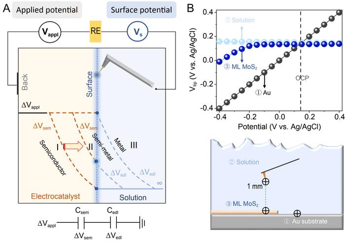
Understanding how voltage drives nanoscale electrocatalysts to initiate reactions is a fundamental scientific question. This is especially challenging when dealing with non-metallic electrocatalysts due to their low inherent carrier concentration, which leads to poor conductivity. When voltage is applied at the non-metal/solution interface, the situation becomes more complex than in the case of metal/solution interfaces. One notable complexity is the significant potential drop within the non-metal, causing the surface potential to often deviate from the back potential. Analyzing the driving force for chemical reactions by applying classical metal models to non-metals can result in substantial inaccuracies. Up until now, distinguishing the potential distribution between the nonmetallic catalyst and the EDL still relies on complex theoretical calculations. The actual potential drop across the semiconductor-electrolyte interface remains unknown, due to the lacks of in in-situ techniques. Moreover, conventional electrochemical characterization only provides the ensemble information for electrode materials, neglecting the spatial heterogeneity in the electronic structures of catalysts. Therefore, a spatially resolved in-situ characterization technique is highly needed.

Credit: ©Science China Press
Understanding how voltage drives nanoscale electrocatalysts to initiate reactions is a fundamental scientific question. This is especially challenging when dealing with non-metallic electrocatalysts due to their low inherent carrier concentration, which leads to poor conductivity. When voltage is applied at the non-metal/solution interface, the situation becomes more complex than in the case of metal/solution interfaces. One notable complexity is the significant potential drop within the non-metal, causing the surface potential to often deviate from the back potential. Analyzing the driving force for chemical reactions by applying classical metal models to non-metals can result in substantial inaccuracies. Up until now, distinguishing the potential distribution between the nonmetallic catalyst and the EDL still relies on complex theoretical calculations. The actual potential drop across the semiconductor-electrolyte interface remains unknown, due to the lacks of in in-situ techniques. Moreover, conventional electrochemical characterization only provides the ensemble information for electrode materials, neglecting the spatial heterogeneity in the electronic structures of catalysts. Therefore, a spatially resolved in-situ characterization technique is highly needed.
In a new research article published in the Beijing-based National Science Review, scientists at Dalian Institute of Chemical Physics, Chinese Academy of Sciences, Xiamen University, University of Chinese Academy of Sciences, Imperial College London autonomously constructed an in-situ surface potential microscope and successfully measured the surface potential of the basal plane of 2H molybdenum disulfide under various voltages. This achievement addresses the experimental challenge of directly measuring the potential distribution at the non-metal/solution interface. The research findings highlight a notable difference in how the surface potential of semiconductors changes with applied voltage compared to metals. When applying voltage from positive to negative, semiconductors shift from maintaining a stable surface potential to displaying variations, gradually resembling the behavior of metals. Scientists further clarified the differences in potential drop values at various applied voltages between the semiconductor (ΔVsem) and the double layer (ΔVedl). They vividly explained how, in a solution environment, the semiconductor’s Fermi level and band structure evolve, demonstrating a transformation of the semiconductor into a highly conductive semimetal.
To further investigate the role of voltage in electrocatalytic reactions, scientists employed atomic force-scanning electrochemical microscopy (AFM-SECM) to study electron transfer (ET) and hydrogen evolution reaction (HER) imaging on molybdenum disulfide. In ET imaging, the semiconductor’s basal plane exhibited strong electron transfer capability, comparable to that of the semimetal edge. However, HER imaging revealed catalytic inertness at the basal plane. Nano-electrochemical imaging results indicated that voltage only affects the ET step. Due to the absence of hydrogen adsorption sites on the basal plane (i.e., chemical sites), voltage cannot drive the electrons on the basal plane to further participate in chemical reactions. This work paves the way for the rational design of efficient nonmetallic electrocatalysts based on the understanding of how voltage acts on nonmetallic catalysts at the nanoscale.
See the article:
Visualizing the role of applied voltage in non-metal electrocatalyst
Natl Sci Rev 2023; doi: 10.1093/nsr/nwad166
https://doi.org/10.1093/nsr/nwad166
Journal
National Science Review
DOI
10.1093/nsr/nwad166


