Scientists in NEXT Lab, Tsinghua University have revealed the fabrication and engineering techniques of TMDs and provided a comparative view between TMDs and traditional semiconductors, demonstrating the benefit of combining TMDs with traditional semiconductors.
Credit: By Zhuofan Chen, Xiaonan Deng, Simian Zhang, Yuqi Wang, Yifei Wu, Shengxian Ke, Junshang Zhang, Fucheng Liu, Jianing Liu, Yingjie Liu, Yuchun Lin, Andrew Hanna, Zhengcao Li, and Chen Wang.
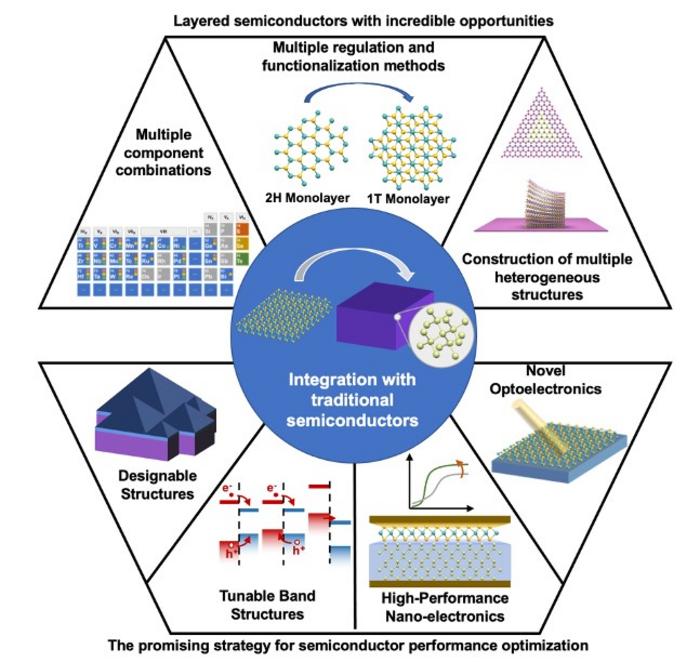
Scientists in NEXT Lab, Tsinghua University have revealed the fabrication and engineering techniques of TMDs and provided a comparative view between TMDs and traditional semiconductors, demonstrating the benefit of combining TMDs with traditional semiconductors.
The research, published in IJEM, shows how to fabricate layered semiconductors modulated with various methods, including phase engineering, defect engineering, doping, and alloying. Then the authors discuss various possibilities to combine layered semiconductors with traditional semiconductors.
Transition metal dichalcogenides (TMDs) with suitable bandgap and band structure have emerged as a new generation of layered semiconductor materials. These advances have demonstrated the immense potential of TMD-based devices in extending Moore’s law to the sub-1 nm scale.
“In principle, this opens up the design of a whole new class of materials in photoelectronic applications, that have exhibited novel properties, such as superconductivity, spin–orbit coupling, ferroelectricity, and ferromagnetism,” said Chen Wang, an associate professor of the School of Materials at the Tsinghua University and the corresponding author on the study. “Essentially, it initiates a new era of devices based on layered materials system with innovative principles,” said Xiaonan Deng (Ph.D. ’21), one of the co-first authors of the paper.
The semiconductor industry has been developing for decades alongside the scaling of device size and increasing density of transistors following the classical Moore’s law. However, the extension of effective Moore’s law has encountered contemporary manufacturing and physics challenges. The most significant physical obstacles impeding the down-scaling of transistors are the short channel effects (SCEs) at several tens of nanometers channel length, and quantum tunneling at sub-10 nm channel lengths.
Due to the 2D nature of layered materials system, heterostructures can be formed among layered materials either laterally via chemical bonds or vertically via van der Waals (vdW) interactions, enabling heterojunction devices based on layered materials. Lateral chemical hetero-integrated junctions offer advantages such as atomically thin interline, mass production process based on chemical reactions, and unique benefits for electronic and optoelectronic devices. On the other hand, vdW heterostructures (vdWHs) can be composed of arbitrary layered materials, offering highly flexible stacking order and angles, as well as naturally atomically sharp interfaces. But the trouble is persisting in the fine synthesis, device performance, and industrial engineering of layered semiconductors, which hampers the widespread utilization of layered-semiconductor-based devices.
In fact, scientists thought as the 2D nature of layered materials system, most processes used in 2D devices are compatible with silicon-based technologies. In addition, the extensive family of layered materials with various band structure, when combined with the well-established band structure of silicon offers a synergistic advantage through heterogeneous integration.
Then, Wang began experimenting with TMDs modulated with various methods, including phase engineering, defect engineering, doping, and alloying.
To the scientists’ astonishment, TMDs enable the exploration of next-generation electronic and optoelectronic devices. “Moreover, vdWHs can be formed by combining different types of layered materials and traditional semiconductors to realize functional devices,” said Simian Zhang (Ph.D. ’21), one of the co-first author. That is enormously helpful for a device that has to function in the real world.
However, what captured the attention of scientists the most was the interface states disorderliness of the novel material’s properties. “Considering the fundamental principles, this should not be plausible for it to function as a semiconductor,” Chen remarked. “Unfortunately, there isn’t a well-established theory that can account for this phenomenon.”
Wang, Chen, and their lab worked with other scientists around the university trying to understand the interface properties of TMDs and traditional semiconductors with various methods. After tests, simulations, and theoretical work, they think that the properties of TMDs can be modulated via phase engineering, defect engineering, doping, and alloying, providing a wide range of alternatives for high-quality layered semiconductors with stable phase and suitable band structure. Besides, non-semiconductor phases of layered semiconductors can be utilized as contacts, dielectrics, and interlayers to build high performance devices, thereby enhancing the technological advantages compared to single-phase silicon materials.
The end result is unprecedented for the layered material. “The research community and industry are actively working to address these challenges in order to facilitate hetero-integration.,” Chen said. The scientists are excited because the discovery suggests a fundamentally new design principle for electronics and optoelectronic technology. Layered materials are so important that virtually any new development opens up new lines for technology, they explained.
One of the material’s attractive characteristics is new options for the formation of heterostructures. For example, the synthesis of WS2-WSe2 and MoS2-MoSe2 lateral heterostructures can be synthesized through step-growth. Vertical heterostructure TMDs can be fabricated using either step growth or mechanical stacking.
The layered semiconductors, represented by atomically thin TMDs with clean vdW interfaces, exhibit excellent controllability and heterogeneous integration potential with other layered materials. Therefore, TMDs based devices were treated as promising candidates for a wide variety of device applications.
Layered semiconductors represented by TMDs show great potential in future electronic and optoelectronic devices. However, despite their extraordinary properties and novel applications, their adoption has been hindered due to the challenges faced in layered semiconductors’ fine synthesis and device engineering.
The team is also exploring the heterogenous integration of layered semiconductors and traditional semiconductors. “We think that the heterogeneous integration between layered and traditional semiconductors, combining the technical and economic advantages of both materials system provides a practical middle route for the early stage of post Moore era,” said Wang.
Wang further concluded, “Although commercialization of layered-traditional heterogeneous integrated devices is yet to be realized, substantial progress has been made in intrinsic physics, material properties, device structures, and integration strategies indicating promising prospects for the future.”
About IJEM:
International Journal of Extreme Manufacturing (IF: 14.7, 1st in the Engineering, Manufacturing category in JCR 2023) is a new multidisciplinary, double-anonymous peer-reviewed and diamond open-access without article processing charge journal uniquely covering the areas related to extreme manufacturing. The journal is devoted to publishing original articles and reviews of the highest quality and impact in the areas related to extreme manufacturing, ranging from fundamentals to process, measurement and systems, as well as materials, structures and devices with extreme functionalities.
Visit our webpage, Like us on Facebook, and follow us on Twitter and LinkedIn.
Journal
International Journal of Extreme Manufacturing
DOI
10.1088/2631-7990/ace501
Article Title
Comparative coherence between layered and traditional semiconductors: unique opportunities for heterogeneous integration
Article Publication Date
15-Jul-2023


