Since the scientists at Bell Labs invented the world’s first transistor in December 1947, a revolution in microelectronics technology has profoundly affected lifestyles worldwide. As electronics get smaller and smaller, it is a challenge to find an easy, fast, and low-cost way to fabricate micro-nano components. Traditional direct writing fabrication methods such as mechanical scribing, focused ion beam etching, electron beam lithography, multiphoton polymerization, and thermal scanning probe etching are inefficient. Although methods such as nanoimprinting, photolithography, plasma etching, and scanning laser interference etching can effectively increase the processing speed, they generally require multiple process steps such as making masks or require very harsh working environments and rely on special Material. Using femtosecond laser to induce surface self-organized periodic structure to manufacture nano-grating structure has attracted people’s attention. Laser-induced periodic surface structures (LIPSS) uses the interference between incident light and surface electromagnetic waves to etch the material, so it has high processing accuracy. Moreover, compared with the traditional laser interference processing method, the self-organized processing method makes its experimental setup simple and scanning with a large light spot makes its fabrication speed rapidly high.
Credit: Liye Xu, Jiao Geng, Liping Shi, Weicheng Cui, Min Qiu
Since the scientists at Bell Labs invented the world’s first transistor in December 1947, a revolution in microelectronics technology has profoundly affected lifestyles worldwide. As electronics get smaller and smaller, it is a challenge to find an easy, fast, and low-cost way to fabricate micro-nano components. Traditional direct writing fabrication methods such as mechanical scribing, focused ion beam etching, electron beam lithography, multiphoton polymerization, and thermal scanning probe etching are inefficient. Although methods such as nanoimprinting, photolithography, plasma etching, and scanning laser interference etching can effectively increase the processing speed, they generally require multiple process steps such as making masks or require very harsh working environments and rely on special Material. Using femtosecond laser to induce surface self-organized periodic structure to manufacture nano-grating structure has attracted people’s attention. Laser-induced periodic surface structures (LIPSS) uses the interference between incident light and surface electromagnetic waves to etch the material, so it has high processing accuracy. Moreover, compared with the traditional laser interference processing method, the self-organized processing method makes its experimental setup simple and scanning with a large light spot makes its fabrication speed rapidly high.
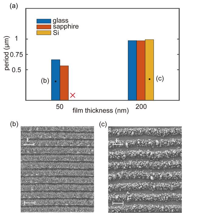
Researchers led by Prof. Min Qiu at Westlake University, China have extensive research experience in LIPSS. They recently discovered that when a periodic grating is induced on the surface of a thin a-Si film, the period of the grating is affected by the interference of incident light with different origins of electromagnetic waves. When the thickness of the amorphous silicon film is small (50 nm) and the substrate is a non-silicon material, LIPSS with a small period is induced under the dominance of the slab waveguide mode. In this case, when the substrate material changes (refractive index changes), the period of the LIPSS also changes. When the thickness of the amorphous silicon film is large (200 nm), the incident light interferes with the quasi-cylindrical wave, and induces the growth of LIPSS under the joint action of near-field and far-field. The period of LIPSS in this mode is slightly smaller than the laser wavelength and is independent of the substrate material. Finite-difference time-domain method-based numerical simulations support the experimental discoveries.
The work entitled “Impact of film thickness in laser-induced periodic structures on amorphous Si films” was published on Frontiers of Optoelectronics (published on Jun. 20, 2023).
Journal
Frontiers of Optoelectronics
DOI
10.1007/s12200-023-00071-6
Article Title
Impact of film thickness in laser-induced periodic structures on amorphous Si films
Article Publication Date
20-Jun-2023


