
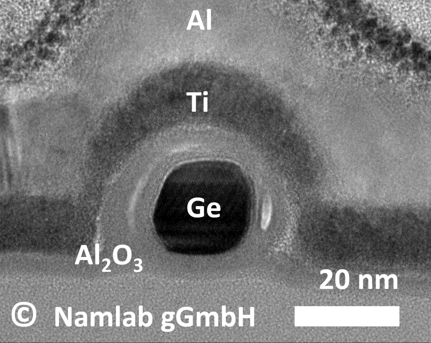
Credit: NaMLab gGmbH
A team of scientists from the Nanoelectronic Materials Laboratory (NaMLab gGmbH) and the Cluster of Excellence Center for Advancing Electronics Dresden (cfaed) at the Dresden University of Technology have demonstrated the world-wide first transistor based on germanium that can be programmed between electron- (n) and hole- (p) conduction. Transistors based on germanium can be operated at low supply voltages and reduced power consumption, due to the low band gap compared to silicon. Additionally, the realized germanium based transistors can be reconfigured between electron and hole conduction based on the voltage applied to one of the gate electrodes. This enables to realize circuits with lower transistor count compared to state-of-the-art CMOS technologies.
Today´s digital electronics are dominated by integrated circuits built by transistors. For more than four decades transistors have been miniaturized to enhance computational power and speed. Recent developments aim to maintain this trend by employing materials having higher mobility than silicon in the transistor channel, like germanium and indium-arsenide. One of the limitations in using those materials is the higher static power loss in the transistor´s off-state, also originating from their small band gaps. The scientist team around Jens Trommer and Dr. Walter Weber from NaMLab in cooperation with cfaed succeeded in solving this issue by conceiving the germanium-nanowire transistor with independent gating regions. Dr. Weber who leads cfaed's Nanowire Research Group points out: "For the first time the results demonstrate the combination of low operation voltages with reduced off-state leakage. The results are a key enabler for novel energy efficient circuits."
The work has been published in the journal ACS Nano.
###
The work has been supported by the German Research Foundation (DFG) in the project ReproNano and has been performed in close cooperation with the DFG Cluster of Excellence Center for Advancing Electronics Dresden (cfaed). NaMLab will strive for further implementation in future products as well as further advancement in R&D with its industrial partners.
Press image caption:
Energy-efficient germanium nanowire transistor with programmable p- and n- conduction. Transmission electron microscope image of cross section.
Download: https://cfaed.tu-dresden.de/files/Images/dynamic/press_releases/2017/namlab_Energy-efficient-germanium-nanowire-transistor.jpg
About NaMLab
The Nanoelectronic Materials Laboratory gGmbH (NaMLab) was founded in July 2006. It is now a non-profit subsidiary company and an associated institute of the TU Dresden. The company runs research facilities with four labs, a clean room and office area for more than 40 scientists and employees on the campus of the TU Dresden. Material research and development combined with the implementation in nano-electronic devices are the goal of NaMLab´s activities. Scientists of NaMLab are closely cooperating with the institutes of the TU Dresden. http://www.namlab.com
About cfaed
cfaed is a microelectronics research cluster of the German Excellence Initiative. It comprises 11 cooperating institutes in Saxony. About 300 scientists from more than 20 countries investigate completely new technologies for electronic information processing. These technologies are inspired by innovative materials such as silicon nanowires, carbon nanotubes or polymers or based on completely new concepts such as the chemical chip or circuit fabrication methods by self-assembling structures e.g., DNA-Origami. The orchestration of these new devices into heterogeneous information processing systems with focus on their resilience and energy-efficiency is also part of cfaed's research program which comprises nine different research paths. http://www.cfaed.tu-dresden.de
Media inquiries:
Matthias Hahndorf'
Technische Universität Dresden
cfaed – Center for Advancing Electronics Dresden
Communications Officer
Tel.: +49 (0) 351 463-42847
[email protected]
Media Contact
Matthias Hahndorf
[email protected]
49-035-146-342-847
@tudresden_de
http://tu-dresden.de/en
############
Story Source: Materials provided by Scienmag

