Semiconductors are indispensable products in our lives, used in everything from smartphones and computers to vehicles. However, their development increasingly poses a problem: as semiconductors improve in terms of function and production volume, the cost to the environment also increases. The greenhouse gases and waste which inevitably arise from the semiconductor manufacturing process have been raised as serious environmental issues, and in the face of the climate crisis, the academic and industrial communities are struggling to cope with them.
Credit: POSTECH
Semiconductors are indispensable products in our lives, used in everything from smartphones and computers to vehicles. However, their development increasingly poses a problem: as semiconductors improve in terms of function and production volume, the cost to the environment also increases. The greenhouse gases and waste which inevitably arise from the semiconductor manufacturing process have been raised as serious environmental issues, and in the face of the climate crisis, the academic and industrial communities are struggling to cope with them.
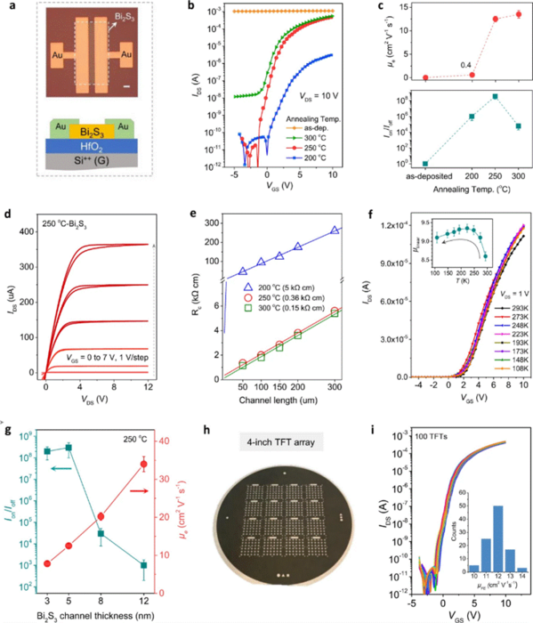
A research team led by Professor Yong-Young Noh and Dr. Ao Liu in the Department of Chemical Engineering at POSTECH has successfully developed high-performance n-type semiconductor of Bi2S3 and p-type Te semiconductor through a simple thermal evaporation process. This technique has attracted attention in that they can be grown over a large area using the thermal evaporating process which is used to manufacture the 8th generation large area OLED (2200 × 2500 mm), in driver circuits of OLED displays, and a variety of semiconductor circuits since it is inexpensive and environmentally friendly.
Metal oxide/polycrystalline silicon (LTPO) currently has the advantage of longer battery life for mobile devices due to its low power consumption, but requires a highly costly and complicated manufacturing process. To meet the growing demands for environmental, social, and governance (ESG) management, a great deal of research has been conducted to develop a more simple and environmentally friendly semiconductor manufacturing process by reducing energy consumption.
Professor Noh’s team decided to use a two-dimensional material, a transition metal chalcogen, which is similar to graphene. Chalcogen refers to sulfur, selenium, and tellurium, which—excluding oxygen—constitute Group 16 on the periodic table of elements. Compounds made of these transition metals have the properties of both conductors and semiconductors. Instead of the conventional solution process, the research team used Bi2S3 to manufacture the thin film of the semiconductor through a thermal evaporation process in which the material is thermally evaporated in a high vacuum and the resulting steam is attached to the board. This process where the quantity of electric charge can be controlled through a simple thermal treatment and semiconductors and conductors can be discretionally manufactured without doping is considered a core proprietary technology of this research.
The research team achieved a high-performance n-type thin film transistor based on this process and also successfully developed a Te high-performance p-type semiconductor in the same way.
In addition, if this transistor and electronic circuit manufacturing process are added in the standard manufacturing process for OLEDs, they may be manufactured through a single-step process. This method will contribute to significantly lowering the high cost of manufacturing OLEDs, which is currently considered one of the disadvantages of the technology.
The budget and manufacturing cost required for the process can also be reduced since the thermal evaporation equipment currently in use for OLEDs may be utilized without new equipment for this process.
Professor Noh who led the research explained, “The Bi2S3 and Te used for this research are very attractive materials that can be transitioned from conductors into semiconductors through a simple thermal treatment. This research was successful in realizing wafer-scale n-type and p-type transistors and the complementary inverter circuit constructed in combination of the two types of transistors through a simple thermal evaporation process, rather than through a costly MOCVD.”
He added, “This research will lead to a variety of additional studies using chalcogen semiconductor devices and commercialization of the related technology.” He also explained his plan, saying “Based on this technology, we are expanding this research into memory devices and neuromorphic devices.”
The study, published in Nature Communications, was supported by the National Research Foundation of Korea and Samsung Display Corporation.
Journal
Nature Communications
DOI
10.1038/s41467-022-34119-6
Article Title
Evaporated nanometer chalcogenide films for scalable high-performance complementary electronics
Article Publication Date
26-Oct-2022


