Background

Credit: by Bangshan Sun
Background
With the advance of semiconductor industry, the traditional electronic integrated circuit is approaching its limit in bandwidth and energy consumption. Compared to electronic integrated circuits, photonic integrated circuits exhibit lower transmission loss, wider bandwidth and smaller time delay. On the other hand, the rapid development of quantum technology in recent decades indicates that quantum chips promise to replace some aspects of traditional electronic integrated circuits in the future.
It is well known that the basic unit of electronic integrated circuit is semiconductor diode. Like electronic integrated circuits, optoelectronic chips or quantum chips have their own basic components. Among these basic components, the micron-scale optical waveguide is one of the most important elements. Based on evanescent wave coupling, adjacent optical waveguides can realize programmable signal processing, providing indispensable functions for the quantum/photonic chips.
Due to previous limitations in fabrication technology, micron-size optical waveguides have been limited to two-dimensional square, elliptic and circular cross-sections. At present, there are limited technology options that can efficiently produce waveguides with both low loss and precise 3D cross-section variation. This imposes many limitations on the functionalities and efficiency of photonic and quantum chips.
The SPIM-WGs Technology
In a new paper published in Light Science & Application, Dr. Bangshan Sun, Prof. Martin J. Booth and a team of scientists at the University of Oxford, collaborated with Prof. Alina Karabchevsky of Israel, Prof. Alexander Jesacher of Austria, and Prof. Ian A. Walmsley of Imperial College London, have developed a new technology named “SPIM-WGs”. With this technique, optical waveguides with continuously variable 3D cross-sections can be efficiently fabricated in a chip. Optical waveguides developed based on this technology not only have superior performance compared to traditional waveguides, but also bring several new features, paving the way for future photonic and quantum chips.
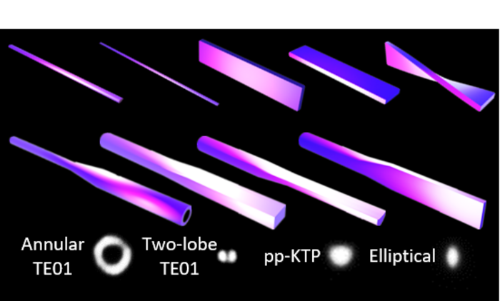
Based on adaptive optics, the technology’s biggest highlight is that it can efficiently produce low-loss waveguides with variable cross-sections, such as circular, square, annular, or many other complicated shapes. The precision in controlling the cross-section in each axis can go down to hundreds of nanometres. For a single waveguide, the shape of cross-section can vary along the waveguide itself. For examples, they can be twisted, varying from square to circular, or from circular to ring shaped, and so on.
It is worth mentioning that the waveguide exhibits very low transmission losses during the precise change of morphology. Based on the glass substrate, the waveguide has a transmission loss of about -0.14 dB/cm, which means that only about 3% of the optical power is lost when transmitting 1 cm through the chip. Experimental results show that the extra transmission loss caused by cross-section variation is almost negligible.
The cost of time to make the waveguides is also noteworthy. For an example, traditional silica-on-silicon (SoS) method takes about a month or more to produce waveguides from preparation. In comparison, SPIM-WGs can be produced in a matter of minutes, which provides a different level of flexibility in prototyping and manufacture.
Application Potential
The most important application of SPIM-WGs is optical mode conversion. In theory, SPIM-WGs can provide the capabilities of optical mode conversion for any arbitrary shapes, limited only by the diffraction limited size of the fabricating laser focus. As shown in the figure, SPIM-WGs can easily convert between Gaussian light modes, elliptical light modes, double lobe TE01, and ring TE01 modes. These modes appear in a wide range of optoelectronic chips.
One most important application in mode conversion is between pp-KTP waveguides and single mode fiber, bridging quantum light sources and quantum chips. At present, the pp-KTP waveguide in quantum light source has to be directly connected to a single-mode fiber, which loses about 25-30% of the light intensity. If the mode conversion waveguide made by SPIM-WGs is used for the bridging, it is expected that the light intensity loss can be reduced below 10%. This would greatly improve the efficiency of most quantum chips.
In addition, based on the functionality of mode conversion, SPIM-WGs can be connected to a single-mode fiber with coupling efficiency up to 95%. This allows SPIM-WGs devices to be easily combined with most existing photonic devices.
It is found that waveguides with rectangular cross-sections twisted at 90 degrees can even be used to control the polarization of light. This also holds great promise for many photonics and quantum applications.
Journal
Light Science & Applications
DOI
10.1038/s41377-022-00907-4


