Single atomic defect is the smallest structural unit of solid material. The construction of devices based on single defect can reach the limit of miniaturization of semiconductor devices. In the past decades, the creation and manipulation of single defects in semiconductors opened a new research field, and could be used to physically realize “qubits” of solid-state quantum computation through spin or electron charge. Most interest have focused on the studies of spin quantum computing. However, the spin manipulation need an optical and magnetic field. On the contrary, multiple charge states can be written and read using only an electric field, which will result in a more compact device size and compatibility with modern electronic technology. A successful charging in single atomic defect needs to overcome Coulomb repulsion energy. The successive multiple charging processes would increase the charging energy quadratically, which easily exceeds the band gap, leading to charging failure. Previous works only observed one or two charging processes.
To manipulate multiple (especially more than two) charge states in solitary defects, a wide band gap with delocalized defect states corresponding to small Coulomb repulsion energy are required. Recently, Jian Gou, Xuguang Wang, Peng Cheng, Kehui Wu from Institute of Physics, Chinese Academy of Sciences, Bingyu Xia, Wenhui Duan, Yong Xu from Tsinghua University, Andrew Wee from National University of Singapore proposed the use of 2D intermetallic semiconductor with delocalized in-gap defect states is a promising solution for the problem of the tradeoff between the band gap and electron delocalization, and made an exciting progress that realized quinary charge states in a single atomic defect.
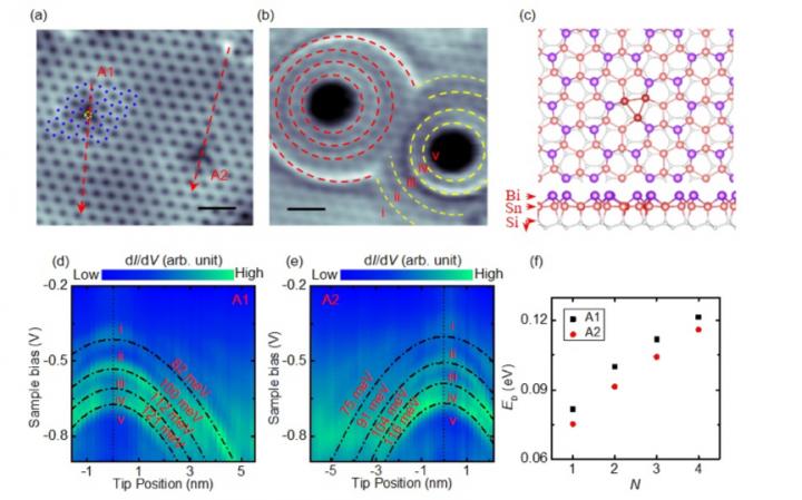
From the perspective of materials design, materials in the two-dimensional (2D) limit can have various chemical stoichiometries and atomic arrangements, thus offering numerous opportunities to construct intermetallic semiconductor which contains two elements that have very close electronegativity. An example is the 2D Sn2Bi layer that grows successfully on Si(111) surface by the same group [PRL 121, 126801(2018)]. The Sn and Bi atoms in this 2D material form an alternating honeycomb structure, in which the valence electrons in both elements are saturated. Consequently, 2D Sn2Bi has a band gap of ~0.8 eV. Meanwhile, due to the very close electronegativity between Sn and Bi, the intrinsic Bi vacancy can possess the strongly delocalized in-gap defect states. Such delocalization can lower the Coulomb energy significantly, when multiple electrons are charging into the single Bi vacancy simultaneously.
Experimentally, the metallic tip in scanning tunneling microscopy (STM) was used to detect the in-gap defect states and inject electrons to defect states. The electric field applied by the STM tip can act as top gate to induce surface band bending, leading to a shift of the in-gap defect states with respect to the Fermi level. The defect states, once aligned with the Fermi level, will be charged. The relative distance variation between the tip and the defect can regulate the Fermi level of Sn2Bi at the defect position. Thus, as shown in the image, when tip is moved across the Bi vacancy, the four charging peaks can be observed and shift to a higher energy with the tip moving always from the defect, representing five charge states transition from zero to four. By fitting the contours, the four charging energies were obtained to be about 100 meV, which is much smaller than the band gap. The growth of charging energy with increasing charge number is not quadratic but sublinear. The ultralow defect charging energy and the sublinear dependence behavior are distinct from typical quadratic charging behaviors of defects.
In theoretical calculations, the Bi vacancy has four in-gap defect states with delocalized distribution, which can result in low defect charge concentration and weak Coulomb repulsion. The simulation of charge energies on the four defect states of Bi vacancy gives the similarly low value and sublinear growth behavior, supporting the discovery and manipulation of quinary charge states in a single atomic defect.
The successful quinary charging in a single atomic defect by the STM tip demonstrates the smallest demo to realize multiple charge states. Single electron can be charged into the Bi vacancy one-by-one controllably and continuously, which presents a more compact unit for the application of solotronics. Meanwhile, the study about the single defect on Sn2Bi shows a paradigm to find other intermetallic semiconductors for more outstanding multiple charge states with low energy in a single atomic defect.
###
See the article:
Jian Gou, Bingyu Xia, Xuguang Wang, Peng Cheng, Andrew Thye Shen Wee,
Wenhui Duan, Yong Xu, Kehui Wu, Lan Chen
National Science Review, nwab070
https:/
Media Contact
Lan Chen
[email protected]
Original Source
http://doi.
Related Journal Article
http://dx.


