Credit: @Science China Press
The rapid development of silicon-based transistors leads to its integration getting closer to the limit of Moore’s law. Graphene is expected to become the next generation of mainstream chip materials due to its ultra-high carrier mobility. However, it is difficult to obtain a high on/off current ratio for intrinsic graphene-based transistor owing to the absence of bandgap. Graphene nanoribbons, which possess a tunable bandgap and unique optoelectrical properties, have attracted extensive attention and exploration.
Nowadays, the preparation of graphene nanoribbons is underdeveloped, and common strategies include the clip of carbon materials (graphene films, carbon nanotubes, or graphite) and direct-growth on a specific substrate surface. All these methods are inspiring but also exhibit narrow scope–they require concession steps to prepare precursors or pre-functionalize substrate as templates. The hundreds of nanometers in length, alignment problem and cumbersome preparation process have retarded the integration of graphene nanoribbons into optoelectronic devices. Therefore, a robust nanotechnology to fabricate GNR with mass production, high quality, and uniform orientation are highly desired for commercialization.
In a new research article published in the Beijing-based National Science Review, scientists at the Institute of Chemistry, Chinese Academy of Sciences, Beijing China and at the Applied Mechanics Laboratory, Department of Engineering Mechanics and Center for Nano and Micro Mechanics, Tsinghua University, Beijing, China, developed a comb-like etching regulated growth process to in-situ fabricate graphene nanoribbon arrays in a template-free CVD system. They also disclosed the growth mechanism by the density functional theory (DFT) based first-principle calculations.
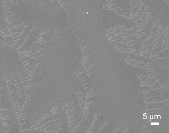
“The introduction of tenuous hydrogen flow is the key factor for realizing the comb-like pattern that promises to achieve the selective growth of graphene nanoribbons in place of the conventional graphene film growth on the liquid Cu surface (Figure 1).” they add. “The distinctive design allows for precisely controlling over width, edge structure, and orientation of graphene nanoribbons.”
To data, the mass production of graphene nanoribbons is limited by the preparation process. “After the in-situ comb-like etching regulated growth process was completed, a large-area GNR array with a uniform orientation was well dispersed over the resolidified Cu surface.” they state.
“The changes of experimental conditions allow for dominating the width and edge structure of graphene nanoribbons, the width decreased to 8 nm with a length of up to 3.1??m (aspect ratio of 387).” Moreover, the as-grown graphene nanoribbons have the smooth and sharp edges with zigzag motif. The scientists demonstrate.
Hydrogen plays a dual role in the formation of graphene by CVD technique. “Owing to the self-limiting growth mechanism, the in-situ formation of graphene nanoribbon arrays operates through stepwise mechanisms, involving an intermediate growth-favored state and a consecutive etching-favored stage. The conversion depends mainly on the catalytic activity of liquid copper surface passivated by as-grown graphene.” they add.
The approach is operationally simple and efficient, offering an assurance for the use of GNR arrays in integrated circuits.
###
This research received funding from the Strategic Priority Research Program of the Chinese Academy of Sciences and the National Natural Science Foundation of China.
See the article:
Le Cai, Wanzhen He, Xudong Xue, Jianyao Huang, Ke Zhou, Xiahong Zhou, Zhiping Xu, and Gui Yu
In situ growth of large-area and self-aligned graphene nanoribbon arrays on liquid metal
National Science Review, nwaa298,
https:/
Media Contact
Gui Yu
[email protected]
Original Source
http://doi.
Related Journal Article
http://dx.


